ISL8014 查看數據表(PDF) - Renesas Electronics
零件编号
产品描述 (功能)
比赛名单
ISL8014 Datasheet PDF : 17 Pages
| |||
ISL8014
Ordering Information
PART NUMBER
(Notes 1, 2, 3)
PART
MARKING
TEMP.
RANGE
(°C)
PACKAGE
(Pb-Free)
PKG.
DWG. #
ISL8014IRZ
80 14IRZ
-40 to +85
16 Ld 4x4 QFN
L16.4x4
NOTES:
1. Add “-T” suffix for tape and reel. Please refer to TB347 for details on reel specifications.
2. These Intersil Pb-free plastic packaged products employ special Pb-free material sets, molding compounds/die attach
materials, and 100% matte tin plate plus anneal (e3 termination finish, which is RoHS compliant and compatible with both
SnPb and Pb-free soldering operations). Intersil Pb-free products are MSL classified at Pb-free peak reflow temperatures that
meet or exceed the Pb-free requirements of IPC/JEDEC J STD-020.
3. For Moisture Sensitivity Level (MSL), please see device information page for ISL8014. For more information on MSL please see
techbrief TB363.
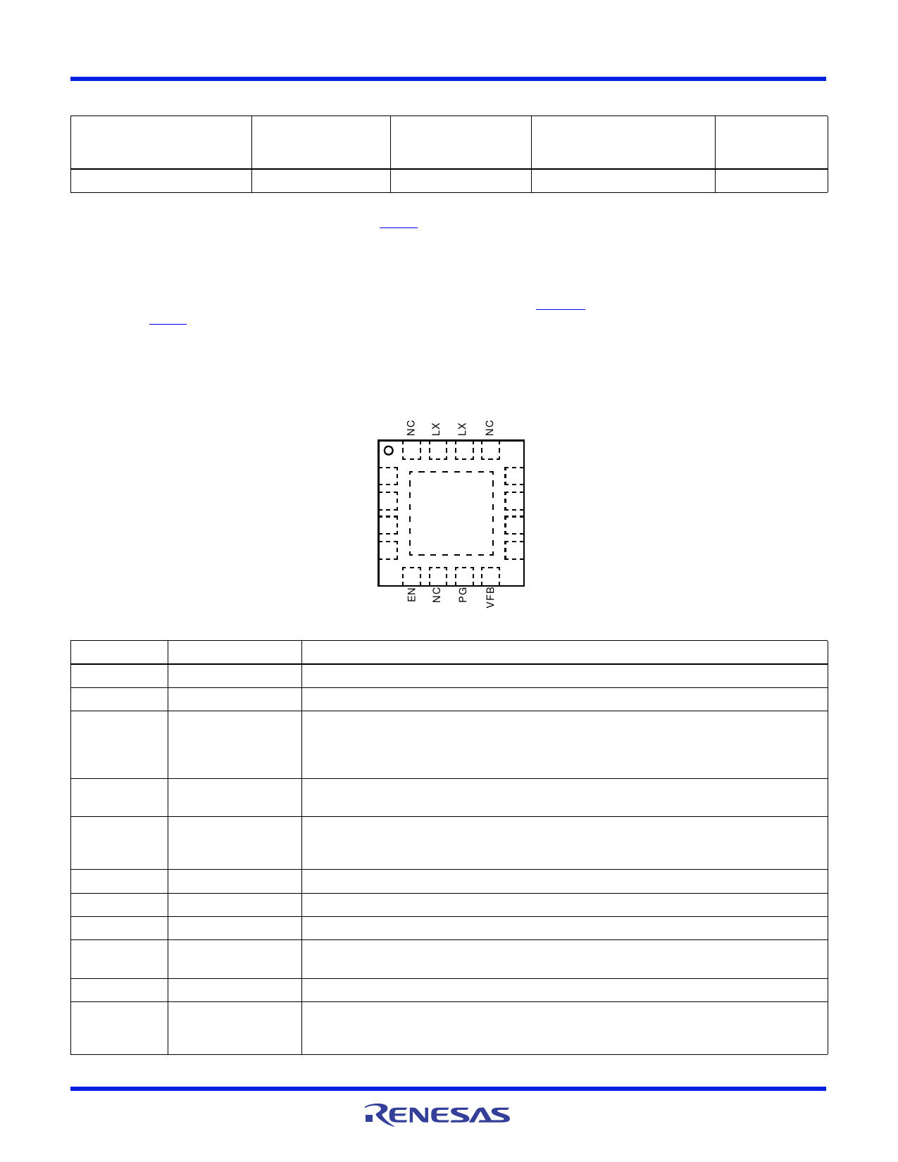
Pin Configuration
ISL8014
(16 LD QFN)
TOP VIEW
16 15 14 13
VIN 1
VIN 2
VDD 3
SYNCH 4
12 PGND
11 PGND
10 SGND
9 SGND
5 678
Pin Descriptions
PIN NUMBER
1, 2
3
5
PIN NAME
VIN
VDD
EN
7
4
14, 15
11, 12
9, 10
8
6, 13, 16
-
PG
SYNCH
LX
PGND
SGND
VFB
NC
Exposed Pad
DESCRIPTION
Input supply voltage. Connect a 10µF ceramic capacitor to power ground.
Input supply voltage for the analog circuitry. Connect to VIN pin.
Regulator enable pin. Keep the EN voltage low in disabled state until VIN settles or is
above 2.5V. Enable the output when driven to high. Shut down the chip and discharge
output capacitor when driven to low. Do not connect directly to VIN or leave this pin
floating.
1ms timer output. At power-up or EN HI, this output is a 1ms delayed Power-Good signal
for the output voltage.
Mode Selection pin. Connect to logic high or input voltage VDD for PWM mode. Connect
to logic low or ground for PFM mode. Connect to an external function generator for
synchronization with the negative edge trigger. Do not leave this pin floating.
Switching node connection. Connect to one terminal of the inductor.
Power ground
Signal ground.
Buck regulator output feedback. Connect to the output through a resistor divider for
adjustable output voltage. For 0.8V output voltage, connect this pin to the output.
No connect.
The exposed pad must be connected to the SGND pin for proper electrical performance.
Place as much vias as possible under the pad connecting to SGND plane for optimal
thermal performance.
FN6576 Rev 4.00
November 23, 2009
Page 2 of 17
Share Link: 