HD74BC374A 查看數據表(PDF) - Renesas Electronics
零件编号
产品描述 (功能)
比赛名单
HD74BC374A Datasheet PDF : 9 Pages
| |||
HD74BC374A
Octal D Type Flip Flops With 3 State Outputs
REJ03D0284–0300Z
(Previous ADE-205-010A (Z))
Rev.3.00
Jul.16.2004
Description
The HD74BC374A provides high drivability and operation equal to or better than high speed bipolar standard logic IC
by using Bi-CMOS process. The device features low power dissipation that is about 1/5 of high speed bipolar logic IC,
when the frequency is 10 MHz. The device has eight edge triger D type flip flop with three state outputs in a 20 pin
package. Data at the D inputs meeting set up reguirements, are transferred to the Q outputs on positive going transitions
of the clock input. When the latch enable goes low, data at the D inputs will be retained at the outputs until latch enable
returns high again. When a high logic level is applied to the output control input, all outputs go to a high impedance
state, regardless of what signals are present at the other inputs and the state of the storage elements.
Features
• Input/Output are at high impedance state when power supply is off.
• Built in input pull up circuit can make input pins be open, when not used.
• TTL level input
• Wide operating temperature range
Ta = –40 to + 85°C
• Ordering Information
Part Name
HD74BC374AFPEL
Package Type Package Code
Package
Abbreviation
SOP-20 pin (JEITA) FP-20DAV
FP
Taping Abbreviation
(Quantity)
EL (2,000 pcs/reel)
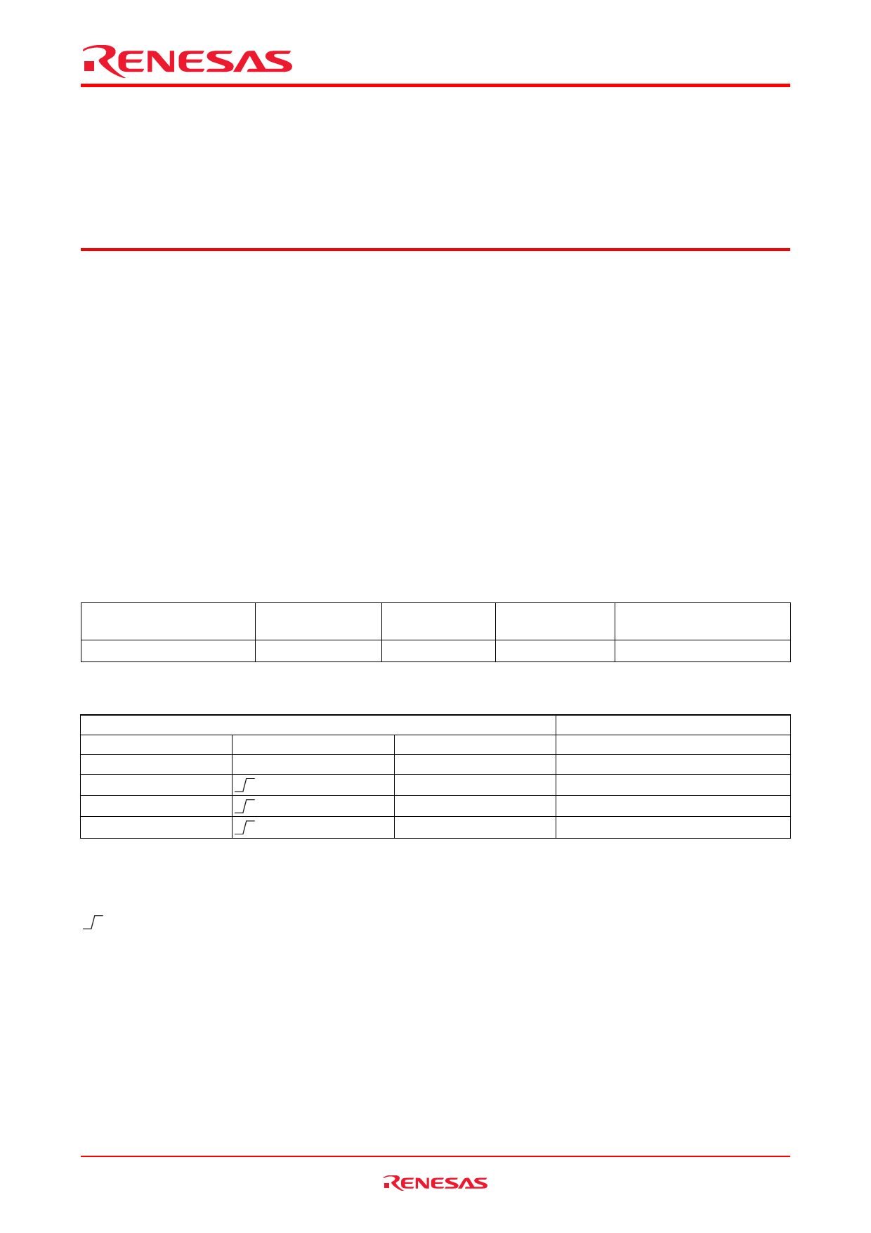
Function Table
Inputs
G
CK
nD
H
X
X
L
L
L
H
L
X
H : High level
L : Low level
X : Immaterial
Z : High impedance
: Low to high transition
Z
L
H
No change
Output
nQ
Rev.3.00, Jul.16.2004, page 1 of 8
Share Link: 