TLE4252G 查看數據表(PDF) - Infineon Technologies
零件编号
产品描述 (功能)
比赛名单
TLE4252G Datasheet PDF : 12 Pages
| |||
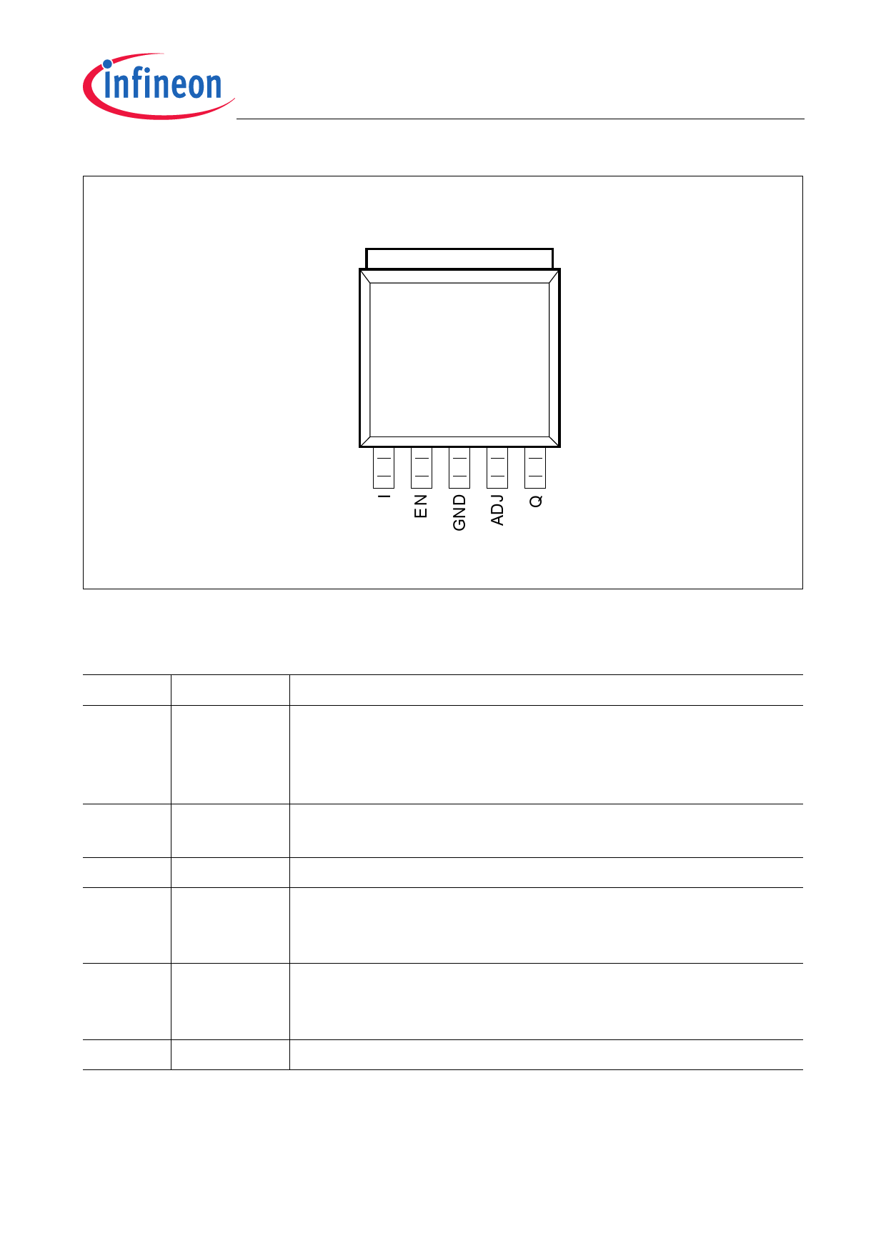
TLE 4252 G
TAB
PG-TO-263 -5
1 23 4 5
TLE4252 G_PINOUT. VSD
Figure 2 Pin Configuration
Table 1
Pin No.
1
2
3
4
5
TAB
Pin Definitions and Functions
Symbol
Function
I
Supply Voltage Input; Input for battery or a pre-regulated
voltage of a e.g. a DC to DC converter.
For compensating line influences, a capacitor to GND close
to the IC pins is recommended.
EN
Enable Input; a high signal turns on the IC, with a low signal
the tracking regulator is turned off.
GND
Ground; connect to TAB.
ADJ
Adjust Input; input for the reference voltage which can be
connected directly or by voltage divider to the reference (see
“Application Information” on Page 8).
Q
Regulator Output; block to GND with a capacitor close to the
IC pins, respecting the values given for its capacitance CQ
and ESR in table “Functional Range” on Page 5.
–
Connect to GND and heatsink area.
Data Sheet
3
Rev. 1.0, 2008-05-09
Share Link: 