LC863256 查看數據表(PDF) - SANYO -> Panasonic
零件编号
产品描述 (功能)
比赛名单
LC863256 Datasheet PDF : 20 Pages
| |||
LC863264/56/48/40A
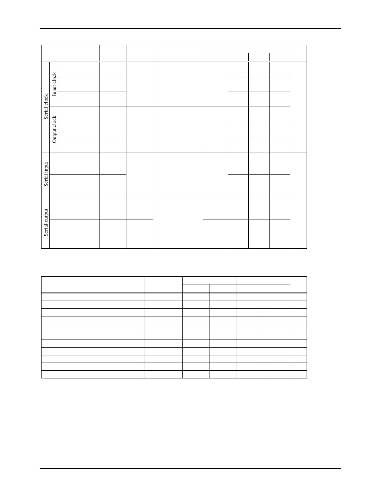
4. Serial Input/Output Characteristics at Ta=-10°C to +70°C, VSS=0V
Parameter
Cycle
Low Level
pulse width
High Level
pulse width
Cycle
Low Level
pulse width
High Level
pulse width
Data set up time
Data hold time
Symbol
Pins
Conditions
tCKCY(1)
tCKL(1)
•SCK0
•SCLK0
Refer to figure 4.
Ratings
unit
VDD[V] min. typ. max.
4.5 - 5.5 2
tCYC
1
tCKH(1)
1
tCKCY(2)
tCKL(2)
•SCK0
•SCLK0
tCKH(2)
•Use pull-up
resistor (1kΩ)
when Nch open-
drain output.
•Refer to figure 4.
4.5 - 5.5
2
1/2tCKCY
1/2tCKCY
tICK
SI0
•Data set-up to
4.5 - 5.5 0.1
µs
SCK0.
•Data hold from
tCKI
SCK0.
0.1
•Refer to figure 4.
Output delay time tCKO(1) SO0
(Using external
clock)
Output delay time tCKO(2) SO0
(Using internal
clock)
•Data hold from
SCK0.
•Use pull-up
resistor (1kΩ)
when Nch open-
drain output.
•Refer to figure 4.
4.5 - 5.5
4.5 - 5.5
7/12tCYC
+0.2
1/3tCYC
+0.2
5. IIC Input/Output Conditions at Ta=-10°C to +70°C, VSS=0V
Parameter
Symbol
Standard
min.
max.
High speed
unit
min.
max.
SCL Frequency
fSCL
0
100
0
400 kHz
BUS free time between stop - start
tBUF
4.7
-
1.3
-
µs
HOLD time of start, restart condition
tHD;STA
4.0
-
0.6
-
µs
L time of SCL
tLOW
4.7
-
1.3
-
µs
H time of SCL
Set-up time of restart condition
tHIGH
4.0
-
0.6
-
µs
tSU;STA
4.7
-
0.6
-
µs
HOLD time of SDA
tHD;DAT
0
-
0
0.9
µs
Set-up time of SDA
tSU;DAT
250
-
100
-
ns
Rising time of SDA, SCL
tR
-
1000 20+0.1Cb 300
ns
Falling time of SDA, SCL
tF
-
300 20+0.1Cb 300
ns
Set-up time of stop condition
tSU;STO
4.0
-
0.6
-
µs
Refer to figure 10
(Note) Cb : Total capacitance of all BUS (unit : pF)
No.6694-12/20
Share Link: 