PI74LCX241 查看數據表(PDF) - Pericom Semiconductor
零件编号
产品描述 (功能)
比赛名单
PI74LCX241 Datasheet PDF : 4 Pages
| |||
PI74LCX241
1122334455667788990011223344556677889900112233445566778899001122112233445566778899001122334455667788990011223344556677889900112211223344556677889900112233445566778899001122334455667788990011221122334455667788990011223344556677889900112233445566778899001122112233445566778899001122
Fast CMOS 3.3V 8-Bit
Buffer/Line Driver
Product Features
• Functionally compatible with FCT3, LVT, and
74 series 241 families of products
• Tri-State outputs
• 5V Tolerant inputs and outputs
• 2.0V-3.6V VCC supply operation
• Balanced sink and source output drives (24 mA)
• Low ground bounce outputs
• Supports live insertion
• ESD Protection exceeds 2000V, Human Body Model
200V, Machine Model
• Packages available:
– 20-pin 209-mil wide plastic SSOP (H)
– 20-pin 173-mil wide plastic TSSOP (L)
– 20-pin 150-mil wide plastic QSOP (Q)
– 20-pin 300-mil wide plastic SOIC (S)
Product Description
Pericom Semiconductor’s PI74LCX series of logic circuits are
produced in the Company’s advanced 0.6 micron CMOS technology
achieving high speed while maintaining low power operation.
The PI74LCX241 is an 8-bit buffer/line driver designed for driving
high capacitive memory loads. With its balanced-drive
characteristics, this high-speed, low power device provides lower
ground bounce, transmission line matching of signals, fewer line
reflections and lower EMI and RFI effects. This makes it ideal for
driving on-board buses and transmission lines.
The PI74LCX241 can be driven from either 3.3V or 5.0V devices
allowing this device to be used as a translator in a mixed
3.3V/5.0V system.
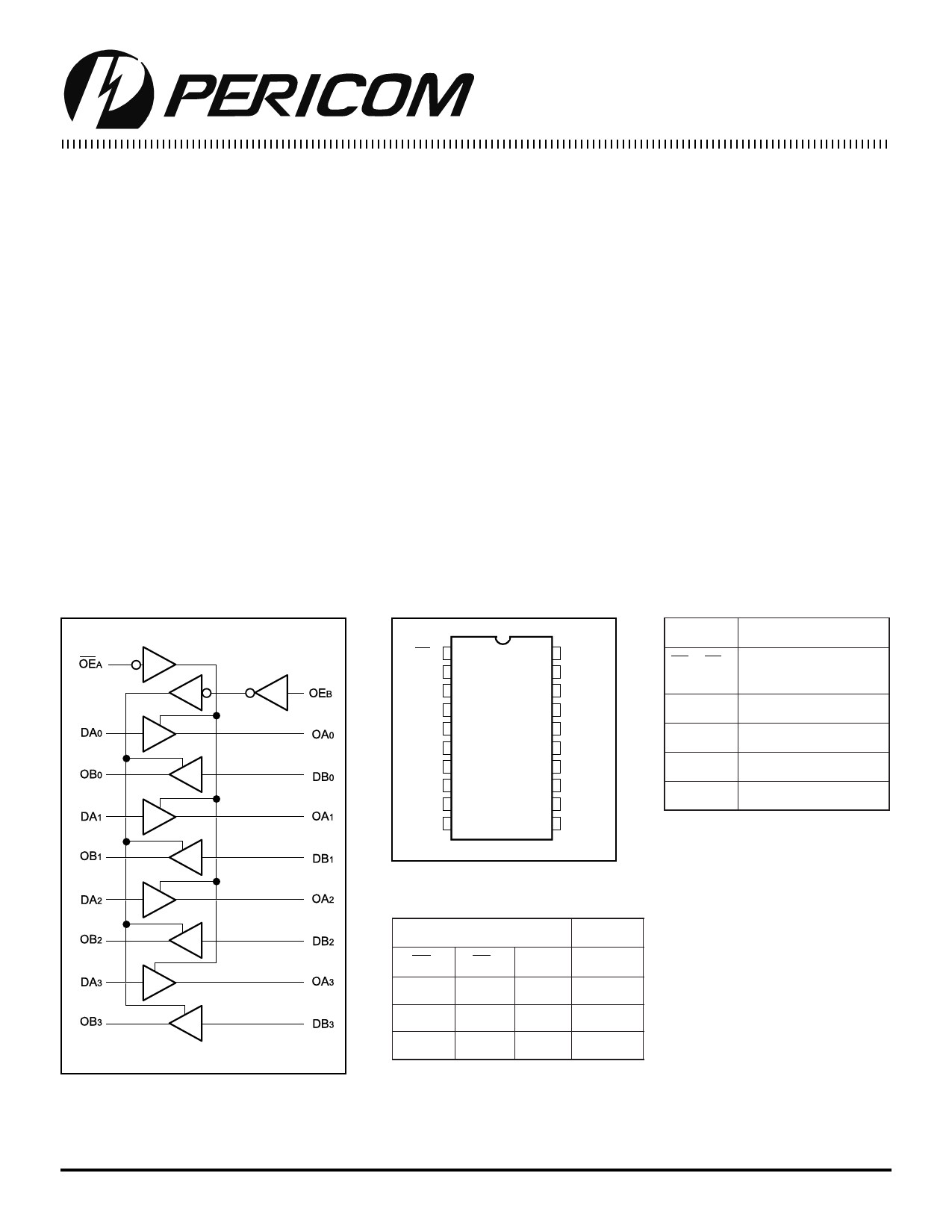
Logic Block Diagram
Product Pin Configuration
OEA 1
20 VCC
DA0 2
19 OEB
OB0 3
18 OA0
DA1 4 20-PIN 17 DB0
OB1 5
DA2 6
OB2 7
DA3 8
H20 16 OA1
L20 15 DB1
Q20
S20
14
OA2
13 DB2
OB3 9
12 OA3
GND 10
11 DB3
Product Pin Description
Pin Name Description
OEA, OEB 3-State Output Enable
Inputs (Active LOW)
DXX
Inputs
OXX
Outputs
GND
Ground
VCC
Power
Truth Table(1)
Inputs
Outputs
OEA
OEB
DXX
OXX
L
H
L
L
L
H
H
H
H
L
X
Z
Note:
1. H = High Voltage Level, X = Don’t Care,
L = Low Voltage Level, Z = High Impedance
1
PS2097A 02/12/97
Share Link: 