AC9248-81 查看數據表(PDF) - Integrated Circuit Systems
零件编号
产品描述 (功能)
比赛名单
AC9248-81 Datasheet PDF : 18 Pages
| |||
ICS9248 -81
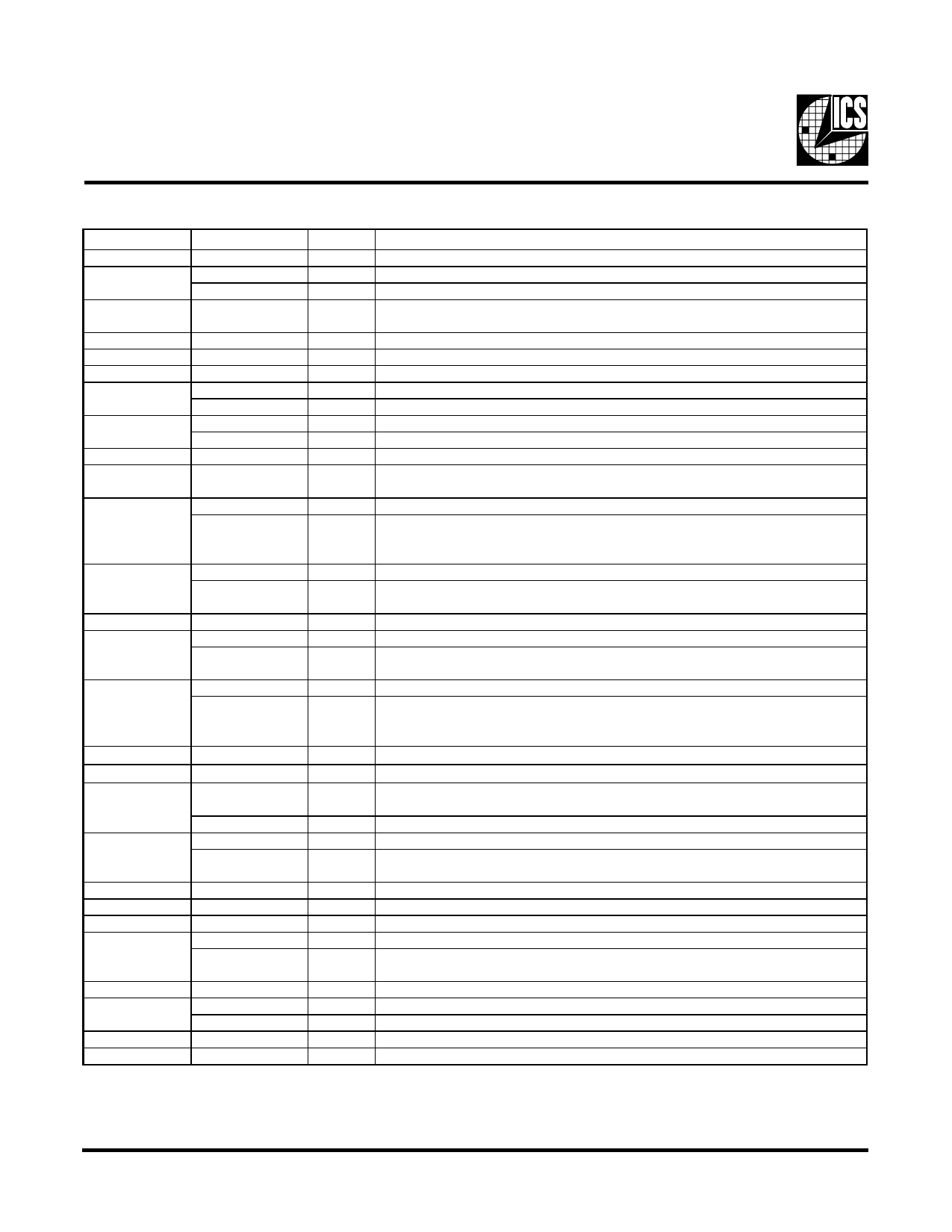
Pin Descriptions
Pin number Pin name Type Description
1
21,2
3,9,16,22,
27,33,39
4
5
6,14
71,2
81,2
13, 12, 11, 10
15,28,29,31,32,
34,35,37,38
17 1
VDDR/X
REF0
Mode
GND
X1
X2
VDDPCI
FS1
PCICLK_F
PCICLK 0
FS2
PCICLK [4:1]
SDRAM 12,
SDRAM [7:0]
SDRAM 11
CPU_STOP#
SDRAM 10
18 1
P CI -S T O P #
19
VDDSD/C
SDRAM 9
20 1
SDRAM_STOP#
SDRAM 8
21 1
PD#
23
24
25 1,2
26 1,2
30,36
40,41,43
42
44 1,2
45
46 1,2
47
48
SDATA
SCLK
SEL24_14#
SIO
FS0
48 MHz
VDDSDR
CPUCLK [3:1]
VDDLCPU
REF2
CPU3.3#_2.5
GNDL
REF1
SD_SEL
IOAPIC
VDDLAPIC
Power
Output
Input
Isolated 3.3 V power for crystal & reference
3.3V, 14.318 MHz reference clock output.
Function select pin, 1=desk top mode, 0=mobile mode. Latched input.
Power 3.3 V Ground
Input
Output
Power
Input
Output
Output
Input
Output
14.318 MHz crystal input
14.318 MHz crystal output
3.3 V power for the PCI clock outputs
Logic input frequency select bit. Input latched at power-on.
3.3 V free running PCI clock output, will not be stopped by the PCI_STOP#
3.3 V PCI clock outputs, generating timing requirements for Pentium II
Logic input frequency select bit. Input latched at power-on.
3.3 V PCI clock outputs, generating timing requirements for Pentium II
Output SDRAM clock outputs. Frequency is selected by SD-Sel latched input.
Output
Input
Output
Input
Power
Output
Input
Output
Input
Input
Input
Input
Output
Input
Output
Power
0utput
Power
Output
Input
Power
Output
Input
Output
Power
SDRAM clock outputs. Frequency is selected by SD-Sel latched input.
Asynchronous active low input pin used to stop the CPUCLK in low state,
all other clocks will continue to run. The CPUCLK will have a "Turnon" latency
of at least 3 CPU clocks.
SDRAM clock outputs. Frequency is selected by SD-SEL latched input.
Synchronous active low input used to stop the PCICLK in a low state. It will not
effect PCICLK_F or any other outputs.
3.3 V power for SDRAM outputs and core
SDRAM clock outputs. Frequency is selected by SD-Sel latched input.
Asynchronous active low input used to stop the SDRAM in a low state.
It will not effect any other outputs.
SDRAM clock outputs. Frequency is selected by SD-Sel latched input.
Asynchronous active low input pin used to power down the device into a low
power state. The internal clocks are disabled and the VCO and the crystal are
stopped. The latency of the power down will not be greater than 3ms.
Data input for I2C serial input.
Clock input of I2C input
This input pin controls the frequency of the SIO. If logic 0 at power on
SIO=14.318 MHz . If logic 1 at power-on SIO=24MHz.
Super I/O output. 24 or 14.318 MHz. Selectable at power-up by SEL24_14MHz
Logic input frequency select bit. Input latched at power-on.
3.3 V 48 MHz clock output, fixed frequency clock typically used with
USB devices
3.3 V power for SDRAM outputs
2.5 V CPU and Host clock outputs
2.5 V power for CPU
3.3V, 14.318 MHz reference clock output.
This pin selects the operating voltage for the CPU. If logic 0 at power on
CPU=3.3 V and if logic 1 at power on CPU=2.5 V operating voltage.
2.5 V Ground for the IOAPIC or CPU
3.3V, 14.318 MHz reference clock output.
This input pin controls the frequency of the SDRAM.
2.5V fixed 14.318 MHz IOAPIC clock outputs
2.5 V power for IOAPIC
Notes:
1: Internal Pull-up Resistor of 120K to 3.3V on indicated inputs
2: Bidirectional input/output pins, input logic levels are latched at internal power-on-reset. Use 10Kohm resistor
to program logic Hi to VDD or GND for logic low.
2
Share Link: 