MC74LCX646DW 查看數據表(PDF) - Motorola => Freescale
零件编号
产品描述 (功能)
比赛名单
MC74LCX646DW Datasheet PDF : 10 Pages
| |||
MC74LCX646
CBA 1
DIR 3
OE 21
SBA 22
SAB 2
CAB 23
A0
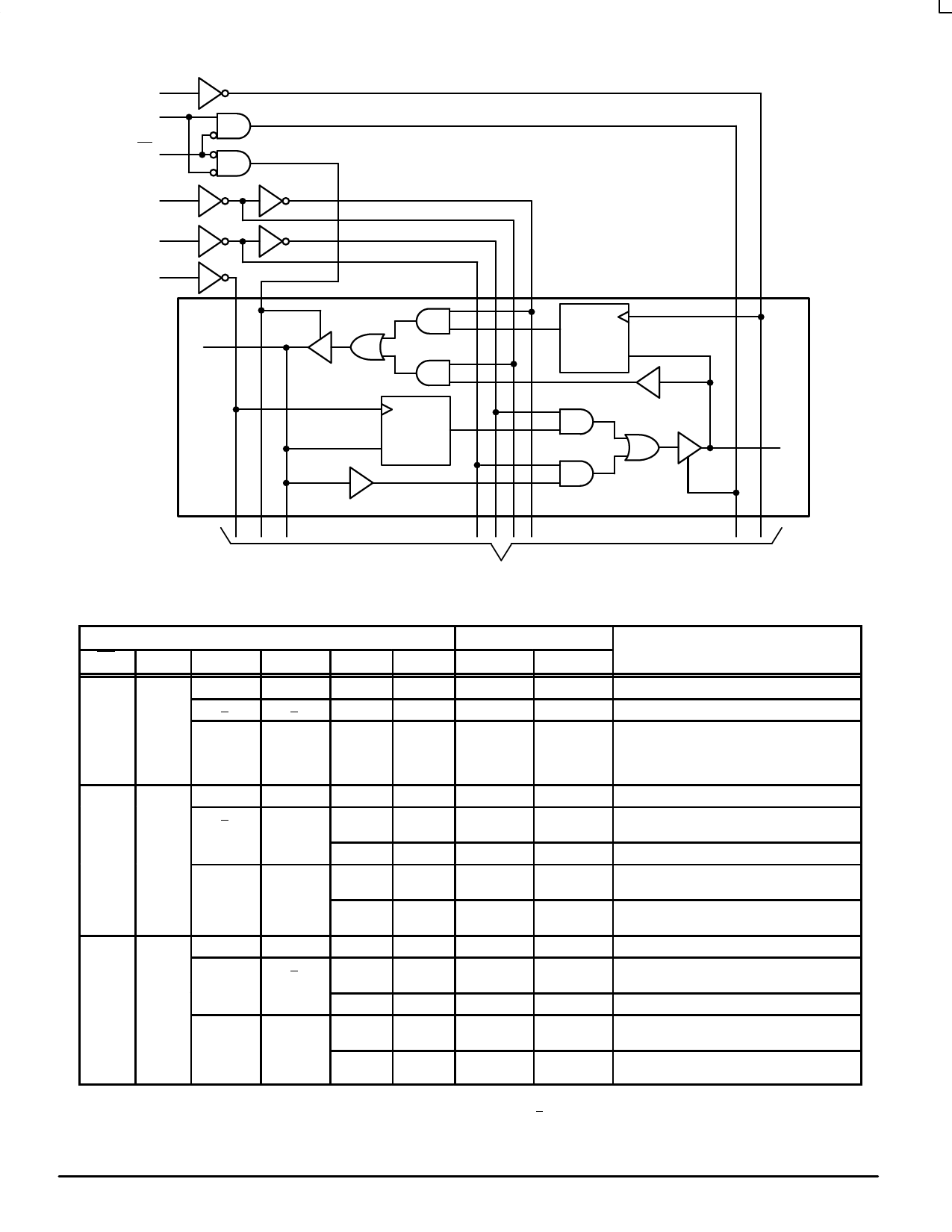
LOGIC DIAGRAM
C
Q
D
C
Q
D
B0
1 of 8 Channels
To 7 Other Channels
FUNCTION TABLE
Inputs
OE
DIR
CAB
CBA
SAB
SBA
Data Ports
An
Bn
Operating Mode
H
X
Input
Input
↑
↑
X
X
X
X
Isolation, Hold Storage
↑
↑
X
X
l
h
X
X
X
Store A and/or B Data
X
l
h
L
H
Input
Output
↑
X*
L
X
L
H
L
Real Time A Data to B Bus
H
H
X
X
QA
Stored A Data to B Bus
↑
X*
L
X
l
h
L
Real Time A Data to B Bus; Store A Data
H
H
X
L
H
QA
Clock A Data to B Bus; Store A Data
QA
L
L
Output
Input
X*
↑
X
L
L
H
L
Real Time B Data to A Bus
H
X
H
QB
X
Stored B Data to A Bus
X*
↑
X
L
L
H
l
Real Time B Data to A Bus; Store B Data
h
X
H
QB
QB
L
Clock B Data to A Bus; Store B Data
H
H = High Voltage Level; h = High Voltage Level One Setup Time Prior to the Low–to–High Clock Transition; L = Low Voltage Level; l = Low Voltage Level One Setup
Time Prior to the Low–to–High Clock Transition; X = Don’t Care; ↑ = Low–to–High Clock Transition; ↑ = NOT Low–to–High Clock Transition; QA = A input storage register;
QB = B input storage register; * = The clocks are not internally gated with either the Output Enables or the Source Inputs. Therefore, data at the A or B ports may be
clocked into the storage registers, at any time. For ICC reasons, Do Not Float Inputs.
MOTOROLA
2
LCX DATA
BR1339 — REV 3
Share Link: 