TGA1319B 查看數據表(PDF) - TriQuint Semiconductor
零件编号
产品描述 (功能)
比赛名单
TGA1319B Datasheet PDF : 5 Pages
| |||
Advance Product Information
January 19, 2001
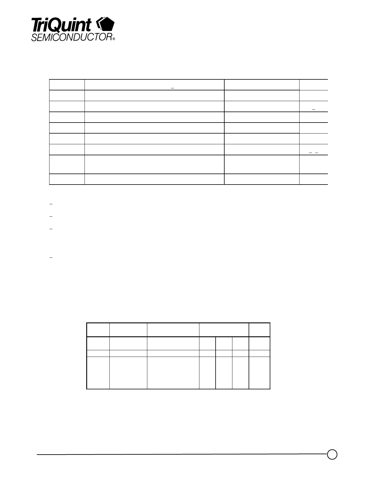
MAXIMUM RATINGS
SYMBOL
V+
I+
I-
PIN
PD
TCH
TM
TSTG
PARAMETER 4/
POSITIVE SUPPLY VOLTAGE
POSITIVE SUPPLY CURRENT
NEGATIVE GATE CURRENT
INPUT CONTINUOUS WAVE POWER
POWER DISSIPATION
OPERATING CHANNEL TEMPERATURE
MOUNTING TEMPERATURE
(30 SECONDS)
STORAGE TEMPERATURE
VALUE
5V
60 mA
5.28 mA
15 dBm
.3 W
150 0C
320 0C
-65 to 150 0C
NOTES
1/
2/ 3/
1/ Total current for all stages.
2/ These ratings apply to each individual FET.
3/ Junction operating temperature will directly affect the device median time to failure (TM). For
maximum life, it is recommended that junction temperatures be maintained at the lowest possible
levels.
4/ These ratings represent the maximum operable values for the device.
ON-WAFER RF PROBE CHARACTERISTICS
(TA = 25 °C ± 5°C)
Vd = 3 V
Symbol Parameter
Test Condition
Gain
NF
PWR
Small Signal
Gain
Noise Figure
Output Power
@ P1dB
F = 21 – 26 GHz
F = 27 GHz
F = 21 – 26.5 GHz
F = 21 GHz
F = 22 GHz
F = 23 – 24 GHz
F = 25 – 26 GHz
F = 27 GHz
Limit
Min Typ Max
18.5
---
17
---
---
2
5
---
6
---
7
---
8
---
10
---
Units
dB
dB
dBm
Note: Devices designated as EPU are typically early in their characterization process prior to finalizing all electrical and process
specifications. Specifications subject to change without notice
TriQuint Semiconductor Texas : Phone (972)994-8465 Fax (972)994 8504 Web: www.triquint.com
2
Share Link: 