HD74HC323 查看數據表(PDF) - Renesas Electronics
零件编号
产品描述 (功能)
比赛名单
HD74HC323 Datasheet PDF : 6 Pages
| |||
HD74HC323
Switching Characteristics
Item
Symbol VCC (V)
Maximum clock
frequency
fmax
2.0
4.5
6.0
Propagation delay tPLH
2.0
time
tPHL
4.5
6.0
2.0
4.5
6.0
Output enable time tZH
2.0
tZL
4.5
6.0
Output disable
time
tHZ
2.0
tLZ
4.5
6.0
Output rise/fall
time
tTLH
2.0
tTHL
4.5
6.0
2.0
4.5
6.0
Input capacitance Cin
—
Ta = 25°C
Min Typ Max
—— 5
— — 27
— — 31
— — 150
— 18 30
— — 26
— — 175
— 20 35
— — 30
— — 150
— 14 30
— — 26
— — 150
— 15 30
— — 26
— — 75
— 5 15
— — 13
— — 60
— 4 12
— — 10
— 5 10
(CL = 50 pF, Input tr = tf = 6 ns)
Ta = –40 to +85°C
Unit
Min
Max
Test Conditions
—
4 MHz
—
21
—
24
—
190 ns Clock to QA’ or QH’
—
38
—
33
—
220 ns Clock to Q
—
44
—
37
—
190 ns
—
38
—
33
—
190 ns
—
38
—
33
—
95
ns QA’, QH’
—
19
—
16
—
75 ns Q
—
15
—
13
—
10 pF
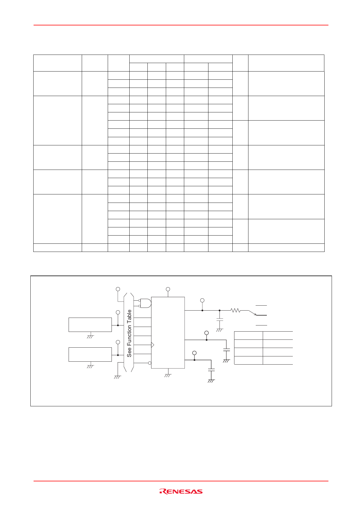
Test Circuit
VCC
VCC
G1
Output
Input
Pulse Generator
G2
G
A/QA
S1 to H/QH
Zout = 50 Ω
S0
Output
1 k Ω S1
CL =
50 pF
OPEN
GND
VCC
Input
Pulse Generator
Zout = 50 Ω
SR
Clock
SL
Clear
QA'
Output CL =
50 pF
QH'
CL =
50 pF
TEST
tPLH / t PHL
tZH/ t HZ
tZL / t LZ
S1
OPEN
GND
VCC
Note : 1. CL includes probe and jig capacitance.
Rev.2.00 Jan 31, 2006 page 4 of 5
Share Link: 