HD74BC541A 查看數據表(PDF) - Renesas Electronics
零件编号
产品描述 (功能)
比赛名单
HD74BC541A Datasheet PDF : 8 Pages
| |||
HD74BC541A
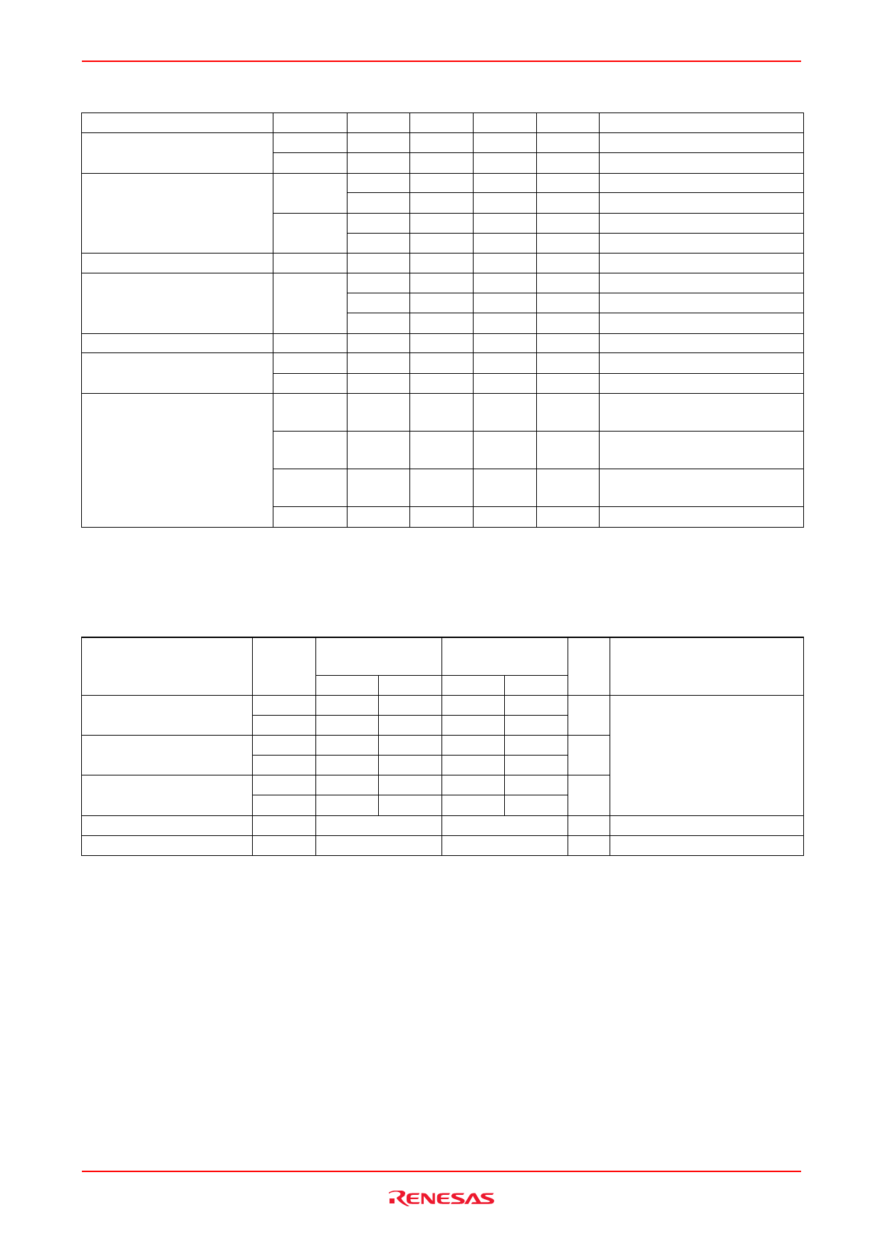
Electrical Characteristics (Ta = –40 to +85°C)
Item
Input voltage
Output voltage
Input diode voltage
Input current
Short circuit output current*1
Off state output current
Supply current
Symbol
VIH
VIL
VOH
VOL
VIK
II
IOS
IOZH
IOZL
ICCL
VCC(V)
4.5
4.5
4.5
4.5
4.5
5.5
5.5
5.5
5.5
5.5
5.5
5.5
Min
2.0
—
2.4
2.0
—
—
—
—
—
—
–100
—
—
—
Max
—
0.8
—
—
0.5
0.55
–1.2
–250
1.0
100
–225
50
–50
29.5
Unit
V
V
V
V
V
V
V
µA
µA
µA
mA
µA
µA
mA
Test Conditions
IOH = –3 mA
IOH = –15 mA
IOL = 48 mA
IOL = 64 mA
IIN = –18 mA
VIN = 0 V
VIN = 5.5 V
VIN = 7.0 V
VIN = 0 or 5.5 V
VO = 2.7 V
VO = 0.5 V
VIN = VCC or GND
All outputs is “L”
ICCH
5.5
—
0.5
mA
VIN = VCC or GND
All outputs is “H”
ICCZ
5.5
—
2.5
mA
VIN = VCC or GND
All outputs is “Z”
ICCT*2
5.5
—
1.5
mA
VIN = 3.4V or 0.5V
Notes: 1. Not more than one output should be shorted at a time and duration of the short circuit should not exceed one
second.
2. When input by the TTL level, it shows ICC increase at per one input pin.
Switching Characteristics (CL = 50 pF)
Item
Propagation delay time
Output enable time
Output disable time
Input capacitance
Output capacitance
Ta = 25°C
Symbol
VCC = 5.0 V
Min
Max
tPLH
3.0
6.0
tPHL
3.0
6.0
tZH
3.0
9.0
tZL
3.0
9.0
tHZ
3.0
8.0
tLZ
3.0
8.0
CIN
3.0 (Typ)
CO
15.0 (Typ)
Ta = –40 to +85°C
VCC = 5.0 V ±10%
Min
Max Unit
Test Conditions
3.0
7.0
ns See under figure
3.0
7.0
3.0
11.0
ns
3.0
11.0
3.0
10.0
ns
3.0
10.0
—
pF VIN = VCC or GND
—
pF VO = VCC or GND
Rev.2.00, Jul.16.2004, page 4 of 7
Share Link: 