CMX631A 查看數據表(PDF) - MX-COM Inc
零件编号
产品描述 (功能)
比赛名单
CMX631A Datasheet PDF : 12 Pages
| |||
Low Voltage SPM Detector
7
CMX631A PRELIMINARY INFORMATION
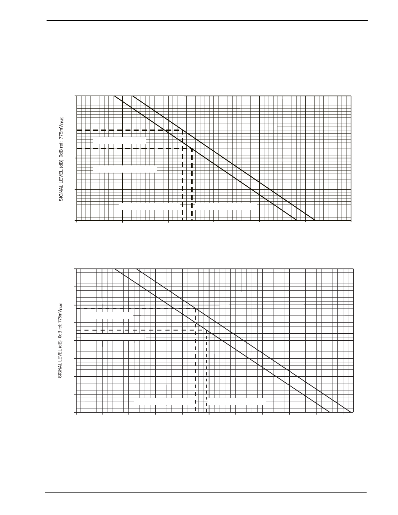
2. Mark the intersection of the upper horizontal line and the upper sloping line; drop a vertical line from this
point to the X-axis [Amplifier Gain (dB)]. The point where the vertical line meets the X-axis indicates the
minimum Input Amp gain required for reliable decoding of valid signals.
3. Mark the intersection of the lower horizontal line and the lower sloping line; drop a vertical line from this
point to the X-axis. The point where the vertical line meets the X-axis will indicate the maximum allowable
Input Amp gain. Input signals at or below the ‘Must-Not’ decode level will not be detected as long as the
amplifier gain is no higher than this level.
-1 0
-2 0
MUST DECODE LEVEL
-3 0
MUST NOT DECODE LEVEL
-4 0
-5 0
-3 0
MINIMUM AMPLIFIER GAIN
MAXIMUM AMPLIFIER GAIN
-2 0
-1 0
0
10
20
AMPLIFIER GAIN (dB) VDD = 3.0V (±0.1) TAMB = -40°C to 85°C
Figure 4: Input Gain Calculation Graph for VDD = 3.0V
-10
-15
-20
MUST DECODE LEVEL
-25
MUST NOT DECODE LEVEL
-30
-35
-40
-45
MINIMUM AMPLIFIER GAIN
MAXIMUM AMPLIFIER GAIN
-50
-25
-20
-15
-10
-5
0
5
10
15
20
AMPLIFIER GAIN (dB) VDD = 5.0 (±0.5) TEMP = -40°C to 85°C
Figure 5: Input Gain Calculation Graph for VDD = 5.0V
30
25
© 1999 MX•COM Inc.
www.mxcom.com Tele: 800 638-5577 336 744-5050 Fax: 336 744-5054
Doc. # 20480177.004
4800 Bethania Station Road, Winston-Salem, NC 27105-1201 USA All trademarks and service marks are held by their respective companies.
Share Link: 