SL23EP08 查看數據表(PDF) - Silicon Laboratories
零件编号
产品描述 (功能)
比赛名单
SL23EP08 Datasheet PDF : 15 Pages
| |||
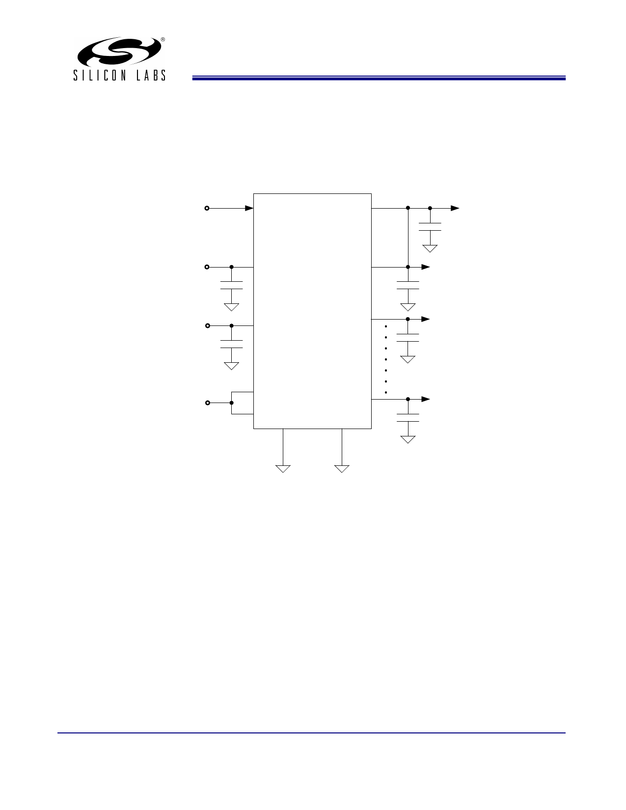
External Components & Design Considerations
Typical Application Schematic
SL23EP08
CLKIN
1
16
VDD
0.1μF
VDD
0.1μF
4
2
SL23EP08
3
13
VDD
S1
9
S2 8 5
GND
11
12
GND
FBK
CL-4pF
CLKA1
CL
CLKA2
CLKB4
CL
Comments and Recommendations
Decoupling Capacitor: A decoupling capacitor of 0.1μF must be used between VDD and VSS pins. Place the capacitor on
the component side of the PCB as close to the VDD pin as possible. The PCB trace to the VDD pin and to the GND via
should be kept as short as possible. Do not use vias between the decoupling capacitor and the VDD pin.
Series Termination Resistor: A series termination resistor is recommended if the distance between the output clocks and
the load is over 1 ½ inch. The nominal impedance of the clock outputs is given on the page 4. Place the series termination
resistors as close to the clock outputs as possible.
Zero Delay and Skew Control: All outputs and CLKIN pins should be loaded with the same load to achieve “Zero Delay”
between the CLKIN and the outputs. The CLKOUT pin is connected to CLKIN internally on-chip for feedback to PLL, and
sees an additional 4 pF load with respect to Bank A and B clocks. For applications requiring zero input/output delay, the load
at the all output pins including the CLKOUT pin must be the same. If any delay adjustment is required, the capacitance at the
CLKOUT pin could be increased or decreased to increase or decrease the delay between Bank A and B clocks and CLKIN.
For minimum pin-to-pin skew, the external load at all the Bank A and B clocks must be the same.
Rev 1.0, May 18, 2006
Page 11 of 15
Share Link: 