ILC7526 查看數據表(PDF) - Fairchild Semiconductor
零件编号
产品描述 (功能)
比赛名单
ILC7526 Datasheet PDF : 7 Pages
| |||
USB Dual Control Switches
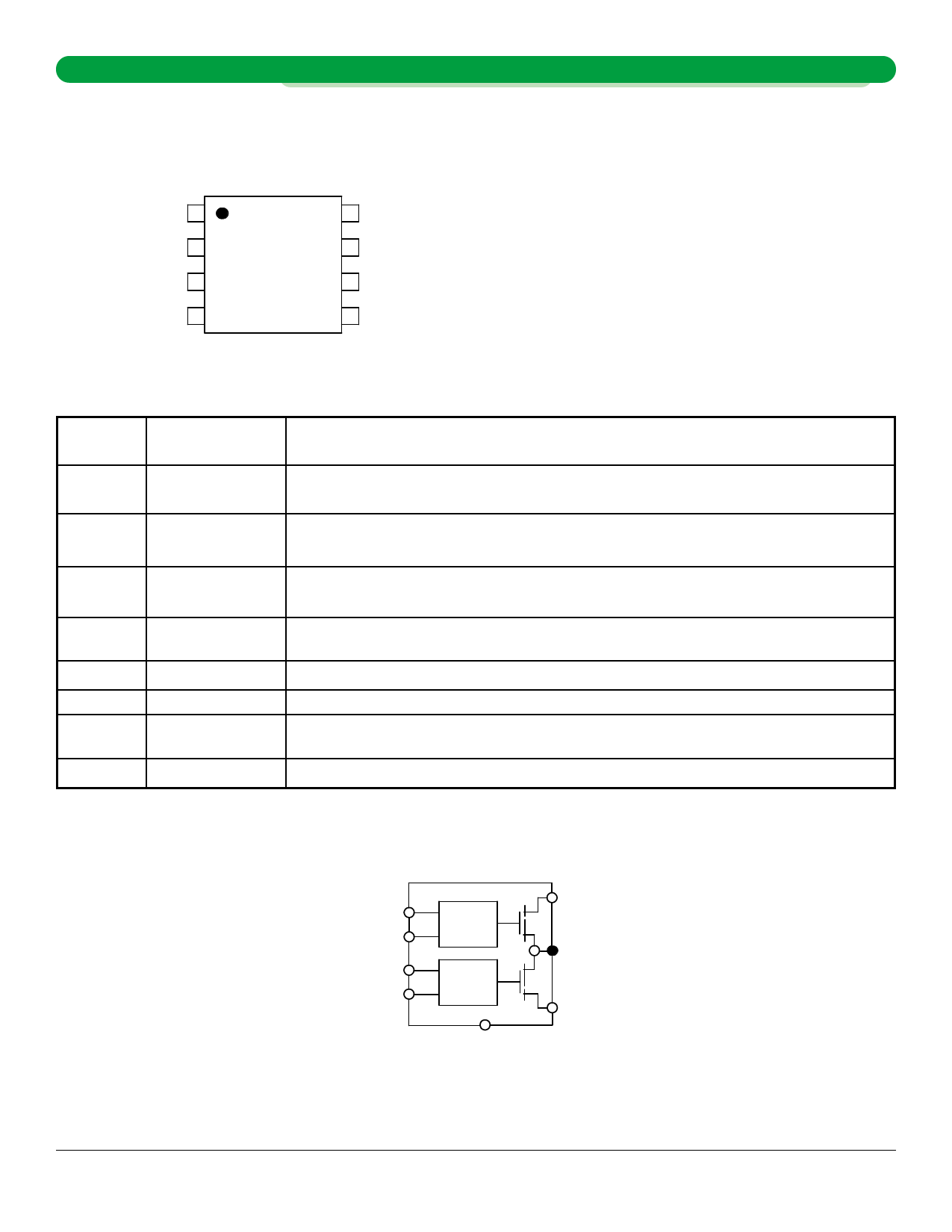
Figure 2: Pin Configuration
ENA 1
FLGA 2
FLGB 3
ENB 4
8 OUTA
7 IN
6 GND
5 OUTB
Preliminary
Pin
Number
1
2
3
4
5
6
7
8
Pin Name
ENA
FLGA
FLGB
ENB
OUTB
GND
IN
OUTA
Pin Description
Enable A (input): Logic-compatible enable input. (7526 active-high, 7536 active-low).
Do not float.
Fault Flag A (Output): Active-low, open-drain output. Indicates overcurrent, UVLO,
or thermal shutdown.
Fault Flag B (Output): Active-low, open-drain output. Indicates overcurrent, UVLO,
or thermal shutdown.
Enable B (Input): Logic-compatible enable input. (7526 active-high, 7536 active-low).
Do not float.
Switch Output B: Output MOSFET source. Typically connect to switched side of load.
Ground: Supply return.
Supply Input: Output MOSFET drain. Also supplies IC’s internal circuitry.
Connect to positive supply.
Switch Output A: Output MOSFET source. Typically connect to switched side of load.
(ENA)1
(FLGA)2
(FLGB)3
(ENB)4
ILC7526
LOGIC
CHARGE
PUMP
LOGIC
CHARGE
PUMP
(GND)6
(OUTA)8
(IN)7
(OUTB)5
2
Rev. 1.6 September 2001
Share Link: 