82C88 查看數據表(PDF) - Renesas Electronics
零件编号
产品描述 (功能)
比赛名单
82C88 Datasheet PDF : 12 Pages
| |||
82C88
Absolute Maximum Ratings
Supply Voltage. . . . . . . . . . . . . . . . . . . . . . . . . . . . . . . . . . . . . +8.0V
Input, Output or I/O Voltage . . . . . . . . . . . . GND -0.5V to VCC +0.5V
ESD Classification . . . . . . . . . . . . . . . . . . . . . . . . . . . . . . . . . Class 1
Operating Conditions
Operating Voltage Range . . . . . . . . . . . . . . . . . . . . . +4.5V to +5.5V
Operating Temperature Range
C82C88 . . . . . . . . . . . . . . . . . . . . . . . . . . . . . . . . . . 0°C to +70°C
I82C88 . . . . . . . . . . . . . . . . . . . . . . . . . . . . . . . . . .-40°C to +85°C
M82C88 . . . . . . . . . . . . . . . . . . . . . . . . . . . . . . . .-55°C to +125°C
Thermal Information
Thermal Resistance (Typical)
JA (°C/W) JC (°C/W)
CERDIP Package. . . . . . . . . . . . . . . .
75
18
CLCC Package . . . . . . . . . . . . . . . . .
85
22
PDIP Package . . . . . . . . . . . . . . . . . .
75
N/A
PLCC Package. . . . . . . . . . . . . . . . . .
75
N/A
Storage Temperature Range . . . . . . . . . . . . . . . . . .-65°C to +150°C
Maximum Junction Temperature
Ceramic Package. . . . . . . . . . . . . . . . . . . . . . . . . . . . . . . . +175°C
Plastic Package . . . . . . . . . . . . . . . . . . . . . . . . . . . . . . . . . +150°C
Maximum Lead Temperature (Soldering 10s) . . . . . . . . . . . . +300°C
(PLCC - Lead Tips Only)
Die Characteristics
Gate Count . . . . . . . . . . . . . . . . . . . . . . . . . . . . . . . . . . . .100 Gates
CAUTION: Stresses above those listed in “Absolute Maximum Ratings” may cause permanent damage to the device. This is a stress only rating and operation of the
device at these or any other conditions above those indicated in the operational sections of this specification is not implied.
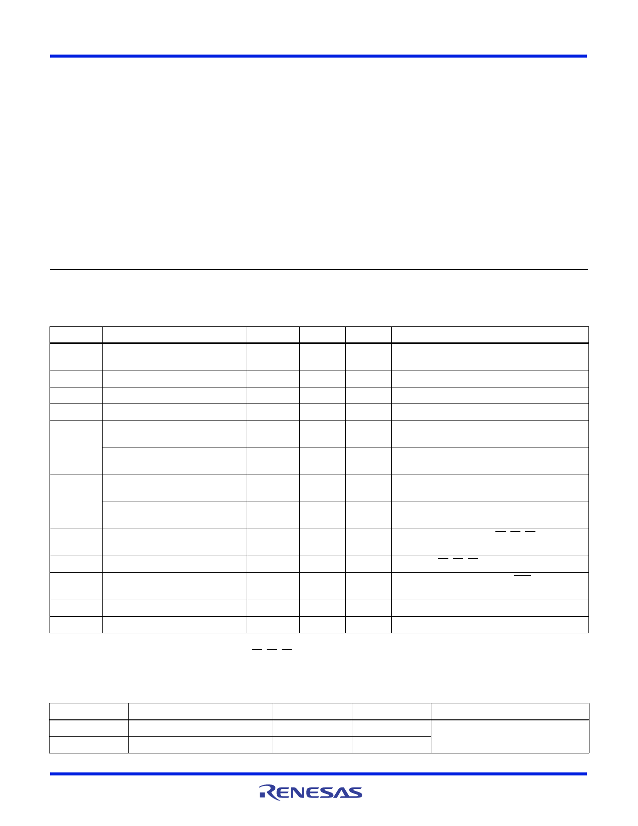
DC Electrical Specifications VCC = 5.0V 10%;
SYMBOL
TA = 0°C to +70°C (C82C88);
TA = -40°C to +85°C (I82C88);
TA = -55°C to +125°C (M82C88)
PARAMETER
MIN
MAX
UNITS
TEST CONDITIONS
VIH
Logical One Input Voltage
2.0
-
V
C82C88, I82C88
2.2
-
V
M82C88
VIL
Logical Zero Input Voltage
-
0.8
V
VIHC CLK Logical One Input Voltage
VCC -0.8
-
V
VILC CLK Logical Zero Input Voltage
-
0.8
V
VOH
VOL
Output High Voltage
Command Outputs
Output High Voltage
Control Outputs
Output Low Voltage
Command Outputs
3.0
-
VCC -0.4
3.0
-
VCC -0.4
-
0.5
V
IOH = -8.0mA
V
IOH = -2.5mA
V
IOH = -4.0mA
V
IOH = -2.5mA
V
IOL= +12.0mA
Output Low Voltage
Control Outputs
-
0.4
V
IOL = +8.0mA
II
Input Leakage Current
-1.0
1.0
A
VIN = GND or VCC, except S0, S1, S2,
DIP Pins 1-2, 6, 15
IBHH
IO
Input Leakage Current-Status Bus
Output Leakage Current
-50
-10.0
-300
10.0
A
VIN = 2.0V, S0, S1, S2 (See Note 1)
A
VO = GND or VCC, IOB = GND, AEN = VCC,
DIP Pins 7-9, 11-14
ICCSB
ICCOP
Standby Power Supply
Operating Power Supply Current
-
10
A
VCC = 5.5V, VIN = VCC or GND, Outputs Open
-
1
mA/MHz VCC = 5.5V, Outputs Open (See Note 2)
NOTES:
1. IBHH should be measured after raising the VIN on S0, S1, S2 to VCC and then lowering to valid input high level of 2.0V.
2. ICCOP = 1mA/MHz of CLK cycle time (TCLCL)
Capacitance TA = +25°C
SYMBOL
PARAMETER
CIN
Input Capacitance
COUT
Output Capacitance
TYPICAL
10
17
UNITS
pF
pF
TEST CONDITIONS
FREQ = 1MHz, all measurements are
referenced to device GND
FN2979 Rev 3.00
August 13, 2015
Page 5 of 12
Share Link: 