CM400DU-5F 查看數據表(PDF) - MITSUBISHI ELECTRIC
零件编号
产品描述 (功能)
比赛名单
CM400DU-5F Datasheet PDF : 4 Pages
| |||
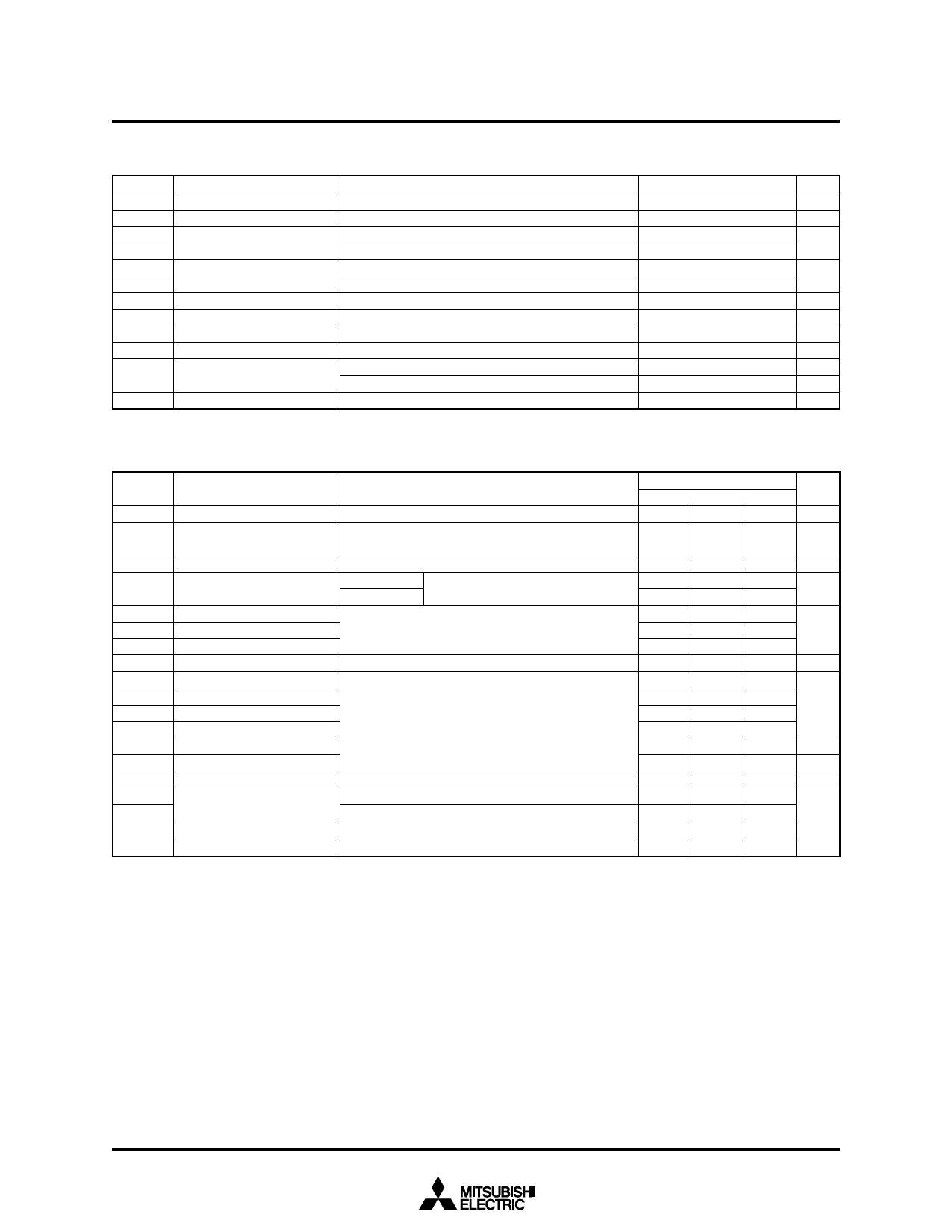
MAXIMUM RATINGS (Tj = 25°C)
Symbol
VCES
VGES
IC
ICM
IE (Note 1)
IEM (Note 1)
PC (Note 3)
Tj
Tstg
Viso
—
—
Parameter
Collector-emitter voltage
Gate-emitter voltage
Collector current
Emitter current
Maximum collector dissipation
Junction temperature
Storage temperature
Isolation voltage
Mounting torque
Weight
G-E Short
C-E Short
TC = 25°C
Pulse
TC = 25°C
Pulse
TC = 25°C
Conditions
Main Terminal to base plate, AC 1 min.
Main Terminal M6
Mounting holes M6
Typical value
MITSUBISHI IGBT MODULES
CM400DU-5F
HIGH POWER SWITCHING USE
(Note 2)
(Note 2)
Ratings
250
±20
400
800
400
800
890
–40 ~ +150
–40 ~ +125
2500
3.5 ~ 4.5
3.5 ~ 4.5
400
Unit
V
V
A
A
W
°C
°C
V
N•m
N•m
g
ELECTRICAL CHARACTERISTICS (Tj = 25°C)
Symbol
Parameter
ICES
Collector cutoff current
Test conditions
VCE = VCES, VGE = 0V
Limits
Min.
Typ.
—
—
VGE(th) Gate-emitter threshold voltage IC = 40mA, VCE = 10V
3.0
4.0
IGES
Gate leakage current
VGE = VCES, VCE = 0V
—
Tj = 25°C
—
VCE(sat) Collector to emitter saturation voltage Tj = 125°C
IC = 400A, VGE = 10V
—
Cies
Input capacitance
—
Coes
Output capacitance
VCE = 10V
—
Cres
Reverse transfer capacitance VGE = 0V
—
QG
Total gate charge
VCC = 100V, IC = 400A, VGE = 10V
—
td(on)
Turn-on delay time
—
tr
Turn-on rise time
VCC = 100V, IC = 400A
—
td(off)
Turn-off delay time
VGE1 = VGE2 = 10V
—
tf
Turn-off fall time
RG = 6.3Ω, Inductive load switching operation
—
trr (Note 1) Reverse recovery time
IE = 400A
—
Qrr (Note 1) Reverse recovery charge
—
VEC(Note 1) Emitter-collector voltage
IE = 200A, VGE = 0V
—
Rth(j-c)Q
Rth(j-c)R
Thermal resistance*1
IGBT part (1/2 module)
FWDi part (1/2 module)
—
—
Rth(c-f)
Contact thermal resistance
Case to fin, Thermal compoundapplied*2 (1/2 module)
—
Rth(j-c’)Q Thermal resistance*3
Tc measured point is just under the chips
—
Note 1. IE, VEC, trr, Qrr and die/dt represent characteristics of the anti-parallel, emitter to collector free-wheel diode. (FWDi).
2. Pulse width and repetition rate should be such that the device junction temp. (Tj) does not exceed Tjmax rating.
3. Junction temperature (Tj) should not increase beyond 150°C.
4. Pulse width and repetition rate should be such as to cause negligible temperature rise.
*1 : Tc measured point is indicated in OUTLINE DRAWING.
*2 : Typical value is measured by using Shin-etsu Silicone “G-746”.
*3 : If you use this value, Rth(f-a) should be measured just under the chips.
—
1.2
1.1
—
—
—
750
—
—
—
—
—
16.0
—
—
—
0.04
—
Max.
1
5.0
0.5
1.7
—
110
7.0
3.8
—
850
400
1100
500
300
—
2
0.14
0.24
—
0.08
Unit
mA
V
µA
V
nF
nC
ns
ns
µC
V
°C/W
Mar. 2002
Share Link: 