IN74HC534A 查看數據表(PDF) - Integral Corp.
零件编号
产品描述 (功能)
比赛名单
IN74HC534A Datasheet PDF : 5 Pages
| |||
IN74HC574A
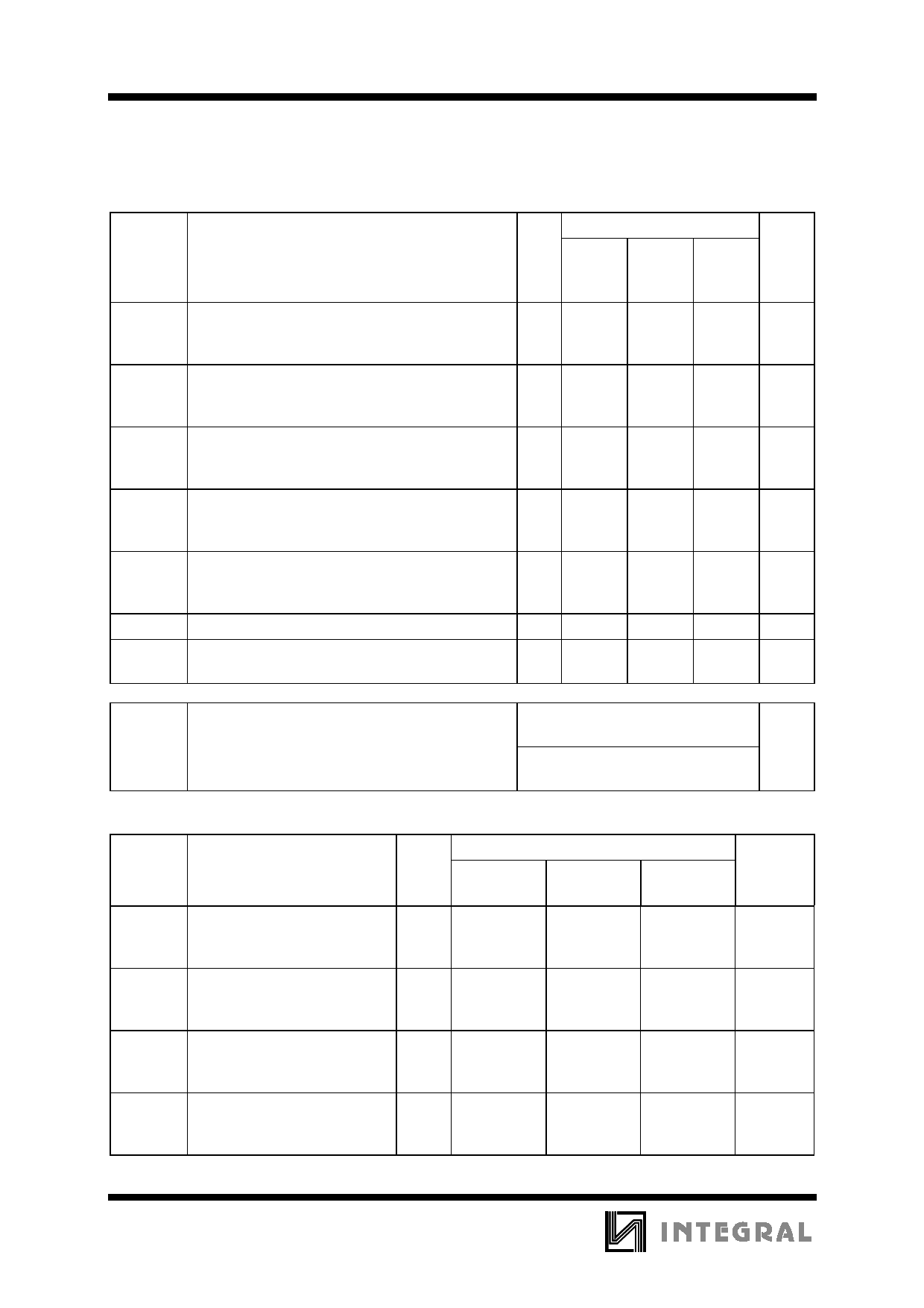
AC ELECTRICAL CHARACTERISTICS(CL=50pF,Input tr=tf=6.0 ns)
Symbol
VCC
Parameter
V
fmax Maximum Clock Frequency (50% Duty Cycle)
2.0
(Figures 1 and 4)
4.5
6.0
tPLH, tPHL Maximum Propagation Delay, Clock to Q
2.0
(Figures 1 and 4)
4.5
6.0
tPLZ, tPHZ Maximum Propagation Delay, Output Enable to Q 2.0
(Figures 2 and 5)
4.5
6.0
tPZH, tPZL Maximum Propagation Delay, Output Enable to Q 2.0
(Figures 2 and 5)
4.5
6.0
tTLH, tTHL Maximum Output Transition Time, Any Output
2.0
(Figures 1 and 4)
4.5
6.0
CIN Maximum Input Capacitance
-
COUT Maximum Three-State Output Capacitance
-
(Output in High-Impedance State)
Guaranteed Limit
25 °C
to
-55°C
≤85°C ≤125°C
6.0
4.8
4.0
30
24
20
35
28
24
160
200
240
32
40
48
27
34
41
150
190
225
30
38
45
26
33
38
140
175
210
28
35
42
24
30
36
60
75
90
12
15
18
10
13
15
10
10
10
15
15
15
Unit
MHz
ns
ns
ns
ns
pF
pF
Power Dissipation Capacitance (Per Enabled
Output)
CPD Used to determine the no-load dynamic power
consumption: PD=CPDVCC2f+ICCVCC
Typical @25°C,VCC=5.0 V
24
TIMING REQUIREMENTS (CL=50pF,Input tr=tf=6.0 ns)
VCC
Symbol
Parameter
V
tSU
Minimum Setup Time, Data to 2.0
Clock (Figure 3)
4.5
6.0
th
Minimum Hold Time, Clock
2.0
to Data (Figure 3)
4.5
6.0
tw
Minimum Pulse Width, Clock 2.0
(Figure 1)
4.5
6.0
tr, tf Maximum Input Rise and Fall 2.0
Times (Figure 1)
4.5
6.0
Guaranteed Limit
25 °C to
-55°C
≤85°C
≤125°C
50
65
75
10
13
15
9
11
13
5
5
5
5
5
5
5
5
5
75
95
110
15
19
22
13
16
19
1000
500
400
1000
500
400
1000
500
400
pF
Unit
ns
ns
ns
ns
416
Share Link: 