SPX2975T5-5.0/TR(2004) 查看數據表(PDF) - Signal Processing Technologies
零件编号
产品描述 (功能)
比赛名单
SPX2975T5-5.0/TR Datasheet PDF : 8 Pages
| |||
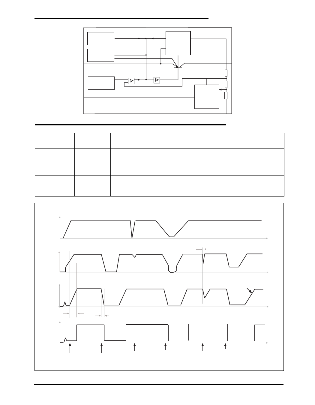
FUNCTIONAL DIAGRAM
Temperature
Sensor
Current
Limit
VIN 1
Bandgap
Reference
4
RD
Saturation
Control &
Protection
Circuit
Buffer
5 VOUT
Reset
Generator
2 RO
3
GND
PIN NUMBER
1
2
3
4
5
PIN DESCRIPTION
PIN NAME
VIN
RO
GND
RD
VOUT
DESCRIPTION
LDO Input. Bypass VIN to GND with a Ceramic capacitor.
Reset Output. RO remains low while VOUT is below the reset switching
threshold. RO is in open conector output.
Ground. This pin also functions as a heatsink. Solder to large pads or the
circuit-board ground plane to maximize thermal dissipation.
Reset Delay. RD connects capacitor to GND for setting delay time.
LDO Output. Bypass VOUT to GND with a minimum 22µF capacitor with
ESR less than 5Ω at 10kHz.
VOUT
VRD
VRO
<Trr
VthH = 1.8V
VthL = 0.4V
Td
Vth = 4.65V
Trr
VROL = 0.2V
Reset Timing
Date: 6/30/04
SPX2975 400mA Low Dropout Voltage Regulator
3
© Copyright 2004 Sipex Corporation
Share Link: 