SPX3940T-L-3-3 查看數據表(PDF) - Exar Corporation
零件编号
产品描述 (功能)
比赛名单
SPX3940T-L-3-3 Datasheet PDF : 11 Pages
| |||
SPX3 9 4 0
1 A Low Dr opou t Volt age Regu lat or
Note 2: Dropout voltage is defined as the input to output differential when the output voltage drops to 99% of its normal
value.
Note 3: Ground pin current is the regulator quiescent current. The total current draw
n from the source is the sum of the
load current to the ground current.
Note 4: VIN =V OUT(NOMINAL) +1V. For example, use V IN =4.3V for a 3.3V regulator. Employ pulse
- testing procedures to minimize
temperature rise.
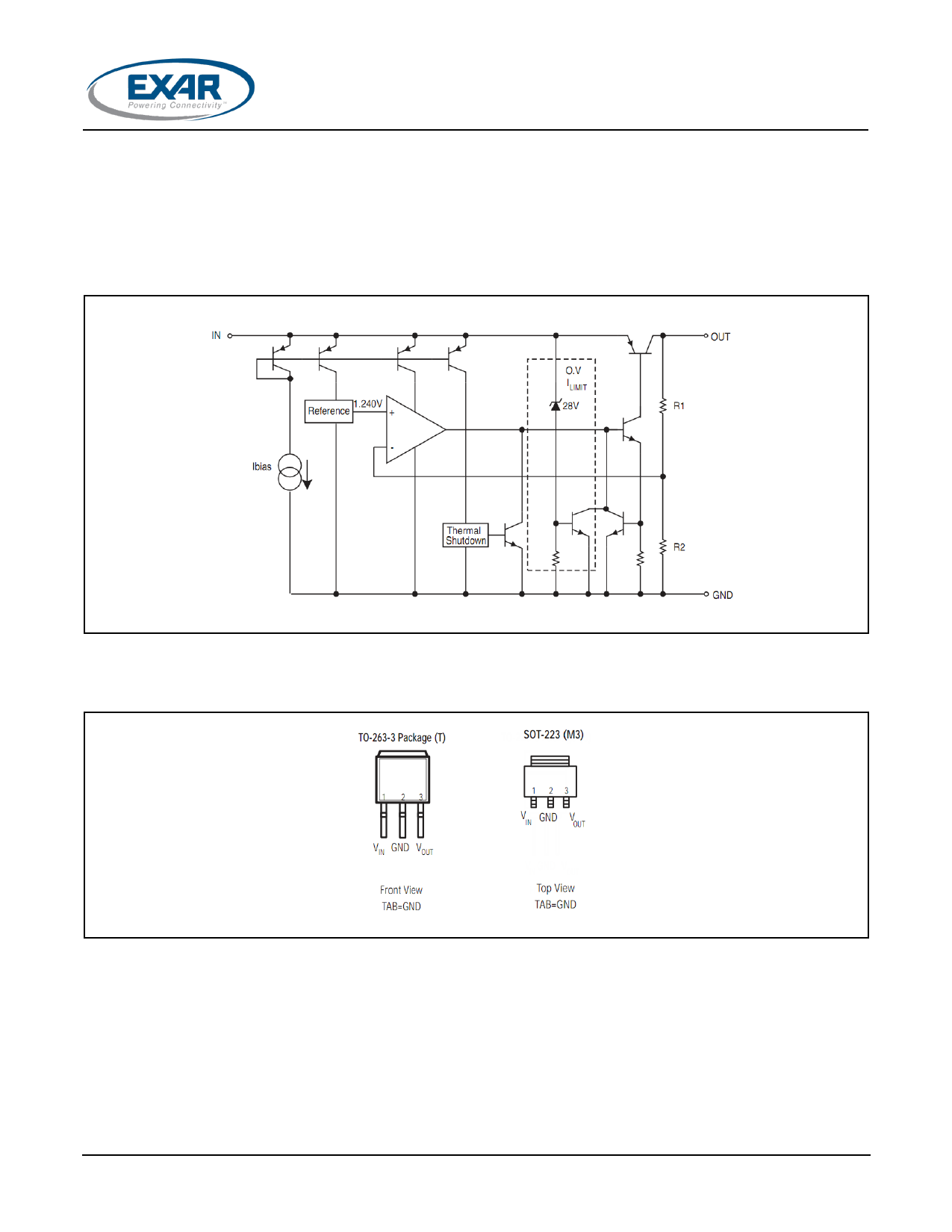
BLOCK DIAGRAM
PIN ASSIGNMENT
Fig. 2: SPX3940 Block Diagram
Fig. 3: SPX3940 Pin Assign ment
© 2012 Exar Corporation
3/ 11
Rev. 1.0.0
Share Link: 