74HC3G06 查看數據表(PDF) - Nexperia B.V. All rights reserved
零件编号
产品描述 (功能)
比赛名单
74HC3G06 Datasheet PDF : 10 Pages
| |||
Nexperia
74HC3G06; 74HCT3G06
Triple inverter with open-drain outputs
Symbol Parameter
Conditions
tPLZ
LOW to OFF-state nA to nY; see Fig. 5
propagation delay
VCC = 2.0 V
VCC = 4.5 V
VCC = 6.0 V
tTHL
HIGH to LOW output nY; see Fig. 5
transition time
VCC = 2.0 V
VCC = 4.5 V
VCC = 6.0 V
CPD
power dissipation VI = GND to VCC
[1]
capacitance
74HCT3G06
tPZL
OFF-state to LOW nA to nY; see Fig. 5
propagation delay
VCC = 4.5 V
tPLZ
LOW to OFF-state nA to nY; see Fig. 5
propagation delay
VCC = 4.5 V
tTHL
HIGH to LOW output VCC = 4.5 V; see Fig. 5
transition time
CPD
power dissipation VI = GND to VCC - 1.5 V [1]
capacitance
-40 °C to +85 °C
Min
Typ
Max
-
24
95
-
11
20
-
10
19
-
18
95
-
6
19
-
5
16
-
4
-
-
9
24
-
12
27
-
6
19
-
4
-40 °C to +125 °C Unit
Min
Max
-
125 ns
-
27 ns
-
23 ns
-
125 ns
-
25 ns
-
20 ns
-
-
pF
-
29 ns
-
32 ns
-
22 ns
-
-
pF
[1] CPD is used to determine the dynamic power dissipation (PD in μW).
PD = CPD × VCC2 × fi × N + Σ(CL × VCC2 × fo) where:
fi = input frequency in MHz;
fo = output frequency in MHz;
CL = output load capacitance in pF;
VCC = supply voltage in V;
N = number of inputs switching;
Σ(CL × VCC2 × fo) = sum of outputs.
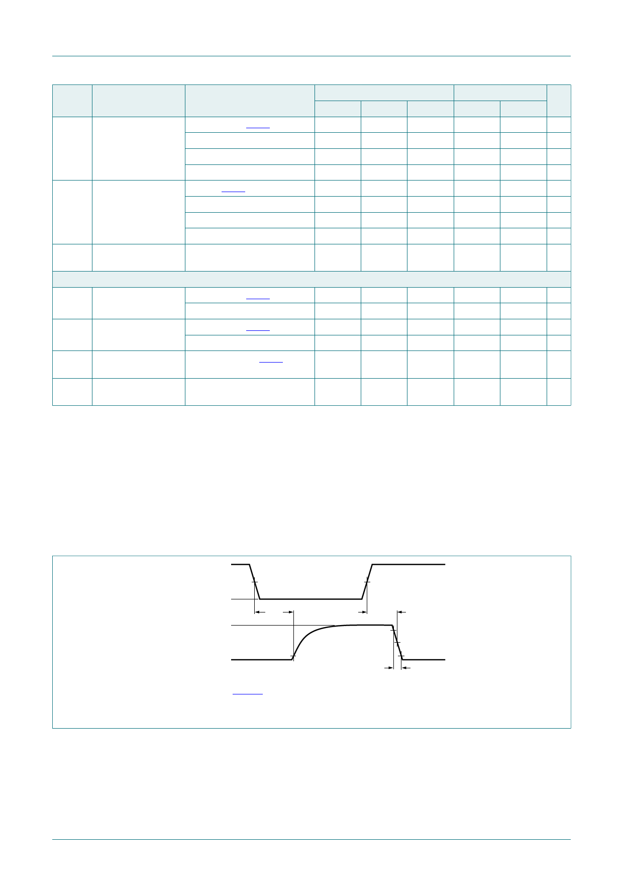
11.1. Waveforms and test circuit
VI
nA input
VM
GND
VCC
tPLZ
tPZL
nY output
VOL
VX
Fig. 5.
Measurement points are given in Table 9.
VOL is the typical output voltage level that occurs with the output load.
The input (nA) to output (nY) propagation delays
VM
tTHL
001aak031
74HC_HCT3G06
Product data sheet
All information provided in this document is subject to legal disclaimers.
Rev. 5 — 1 May 2019
© Nexperia B.V. 2019. All rights reserved
5 / 10
Share Link: 