ISL81483 查看數據表(PDF) - Renesas Electronics
零件编号
产品描述 (功能)
比赛名单
ISL81483
Renesas Electronics

ISL81483 Datasheet PDF : 14 Pages
| |||
ISL8487, ISL81483, ISL81487
Pin Descriptions
PIN
FUNCTION
RO
Receiver output: If A > B by at least 0.2V, RO is high; If A < B by 0.2V or more, RO is low; RO = High if A and B are unconnected (floating).
RE
Receiver output enable. RO is enabled when RE is low; RO is high impedance when RE is high.
DE
Driver output enable. The driver outputs, Y and Z, are enabled by bringing DE high. They are high impedance when DE is low.
DI
Driver input. A low on DI forces output Y low and output Z high. Similarly, a high on DI forces output Y high and output Z low.
GND Ground connection.
A/Y
RS-485/422 level, noninverting receiver input and noninverting driver output. Pin is an input (A) if DE = 0; pin is an output (Y) if DE = 1.
B/Z
RS-485/422 level, inverting receiver input and inverting driver output. Pin is an input (B) if DE = 0; pin is an output (Z) if DE = 1.
VCC System power supply input (4.5V to 5.5V).
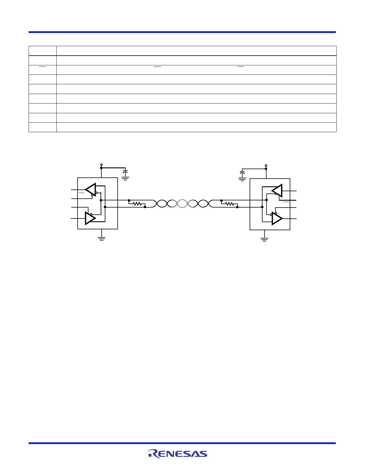
Typical Operating Circuits
+5V
+
8
0.1F
VCC
1 RO R
2 RE
B/Z 7
RT
3 DE
A/Y 6
4 DI D
GND
5
ISL8487, ISL81483, ISL81487
+5V
0.1F +
RT
7
6
8
VCC
B/Z
A/Y
D DI 4
DE 3
RE 2
R
GND
5
RO 1
FN6050 Rev 8.00
March 14, 2016
Page 3 of 14
Share Link: