ISL85001 查看數據表(PDF) - Renesas Electronics
零件编号
产品描述 (功能)
比赛名单
ISL85001 Datasheet PDF : 16 Pages
| |||
ISL85001
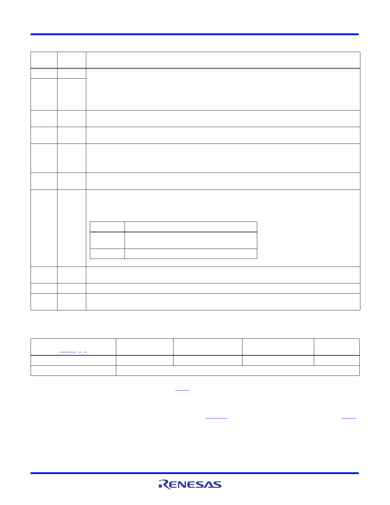
Pin Descriptions
SYMBOL
FB
COMP
SS
EN
PG
GND
VDD
PIN
NUMBER
DESCRIPTION
1
The standard buck regulator employs a single voltage control loop. FB is the negative input to the voltage loop error amplifier.
COMP is the output of the error amplifier. The output voltage is set by an external resistor divider connected to FB. With a
2
properly selected divider, the output voltage can be set to any voltage between the power rail (reduced by converter losses) and
the 0.6V reference. Connecting an AC network across COMP and FB provides loop compensation to the amplifier.
In addition, the PWM regulator power-good and undervoltage protection circuitry use FB to monitor the regulator output
voltage.
3
Program pin for soft-start duration. A regulated 30µA pull-up current source charges a capacitor connected from the pin to
GND. The output voltage of the converter follows the ramping voltage on the SS pin.
4
PWM controller enable input. The PWM converter output is held off when the pin is pulled to ground. When the voltage on this
pin rises above 1.7V, the chip is enabled.
5
PWM converter power-good output. Open drain logic output that is pulled to ground when the output voltage is outside
regulation limits. Connect a 100kΩ resistor from this pin to VDD. Pin is low when the buck regulator output voltage is not within
10% of the respective nominal voltage, or during the soft-start interval. Pin is high impedance when the output is within
regulation.
6
Ground connect for the IC and thermal relief for the package. The exposed pad must be connected to GND and soldered to the
PCB. All voltage levels are measured with respect to this pin.
7
Internal 5V linear regulator output provides bias to all the internal control logic. The ISL85001 may be powered directly from a 5V
(±10%) supply at this pin. When used as a 5V supply input, this pin must be externally connected to VIN. The VDD pin must always
be decoupled to GND with a ceramic bypass capacitor (minimum 1µF) located close to the pin.
TABLE 1. INPUT SUPPLY CONFIGURATION
INPUT
PIN CONFIGURATION
5.5V to 25V Connect the input supply to the VIN pin only. The VDD pin will
provide a 5V output from the internal linear regulator.
5V ±10% Connect the input supply to the VIN and VDD pins.
BOOT
PHASE
VIN
8
9, 10
11, 12
Floating bootstrap supply pin for the power MOSFET gate driver. The bootstrap capacitor provides the necessary charge to turn
and hold on the internal N-channel MOSFET. Connect an external capacitor from this pin to PHASE.
Switch node connections to internal power MOSFET source, external output inductor and external diode cathode.
The input supply for the PWM regulator power stage and the source for the internal linear regulator that provides bias for the
IC. Place a ceramic capacitor from VIN to GND, close to the IC for decoupling (typical 10µF).
Ordering Information
PART NUMBER
(Notes 1, 2, 3)
PART
MARKING
TEMP. RANGE
(°C)
PACKAGE
(RoHS COMPLIANT)
PKG.
DWG. #
ISL85001IRZ
501Z
-40 to +85
12 Ld DFN
L12.4x3
ISL85001EVAL1Z
Evaluation Board
NOTES:
1. Add “-T” suffix for 6k unit tape and reel option. Please refer to TB347 for details on reel specifications.
2. These Intersil Pb-free plastic packaged products employ special Pb-free material sets, molding compounds/die attach materials, and 100% matte
tin plate plus anneal (e3 termination finish, which is RoHS compliant and compatible with both SnPb and Pb-free soldering operations). Intersil
Pb-free products are MSL classified at Pb-free peak reflow temperatures that meet or exceed the Pb-free requirements of IPC/JEDEC J STD-020.
3. For Moisture Sensitivity Level (MSL), please see device information page for ISL85001. For more information on MSL please see tech brief TB363.
FN6769 Rev.3.00
Apr 14, 2017
Page 4 of 16
Share Link: 