ISL976787IBZ 查看數據表(PDF) - Renesas Electronics
零件编号
产品描述 (功能)
比赛名单
ISL976787IBZ
Renesas Electronics

ISL976787IBZ Datasheet PDF : 24 Pages
| |||
ISL97687
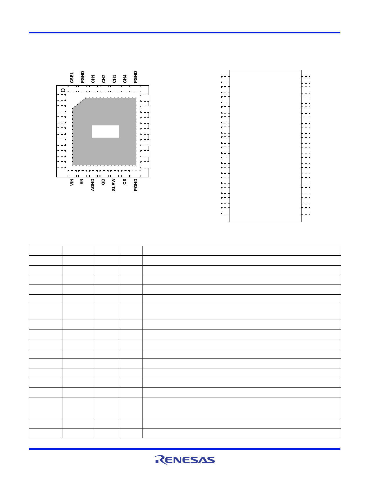
Pin Configurations
ISL97687
(28 LD 5x5 TQFN)
TOP VIEW
PWMI 1
28 27 26 25 24 23 22
21 ACTL
STV 2
20 OSC
EN_ADIM 3
EN_PS 4
VLOGIC 5
THERMAL*
PAD
19 ISET2
18 ISET1
17 COMP
EN_VSYNC 6
16 OVP
VDC 7
15 PWM_SET/PLL
8 9 10 11 12 13 14
*EXPOSED THERMAL PAD
CH2 1
CH1 2
PGND 3
CSEL 4
PWMI 5
STV 6
EN_ADIM 7
EN_PS 8
VLOGIC 9
EN_VSYNC 10
VDC 11
VIN 12
EN 13
AGND 14
ISL97687
(28 LD SOIC)
TOP VIEW
28 CH3
27 CH4
26 PGND
25 ACTL
24 OSC
23 ISET2
22 ISET1
21 COMP
20 OVP
19 PWM_SET/PLL
18 PGND
17 CS
16 SLEW
15 GD
Pin Descriptions
TQFN
1
2
3
4
5
6
7
8
9
10
11
12
13
14
15
16
17
SOIC
5
6
7
8
9
10
11
12
13
14
15
16
17
18
19
20
21
PIN NAME PIN TYPE
PIN DESCRIPTION
PWMI
I PWM Brightness Control Input pin.
STV
I Start Vertical Frame signal; used in VSYNC mode.
EN_ADIM
I Enable Analog Dimming
EN_PS
I Enable Phase Shift
VLOGIC
S Internal 2.5V Digital Bias Regulator. Needs Decoupling Capacitor added to ground.
EN_VSYNC
I
Frame synchronization enable. Ties high to VDC for enable VSYNC function. PWM_SET/PLL also
needs to be configured with an RC network. Pin can be tied to VDC or VLOGIC to enable function.
VDC
S Internal 5V Analog Bias Regulator. Needs Decoupling Capacitor added to ground.
VIN
S Main Power Input. Range: 9V to 32V.
EN
I LED Driver Enable. Whole chip will shut down when low.
AGND
S Analog Ground
GD
O External Boost FET gate control
SLEW
I Boost Regulation Switching Slew Rate control.
CS
I External Boost FET current sense input.
PGND
S Boost FET gate driver power ground and ground reference for CS pin.
PWM_SET/ I For direct PWM mode, tie this pin high to VDC. For other non-VSYNC modes, connect to a resistor
PLL
to set the dimming frequency. If the VSYNC function is enabled, connect this pin to the PLL loop
filter network.
OVP
I Overvoltage Protection Input as well as Output Voltage feedback pin.
COMP
I Boost compensation
FN7714 Rev.3.00
Sep 13, 2017
Page 3 of 24
Share Link: