STW13NK60Z(2005) 查看數據表(PDF) - STMicroelectronics
零件编号
产品描述 (功能)
比赛名单
STW13NK60Z
(Rev.:2005)
(Rev.:2005)
STMicroelectronics

STW13NK60Z Datasheet PDF : 17 Pages
| |||
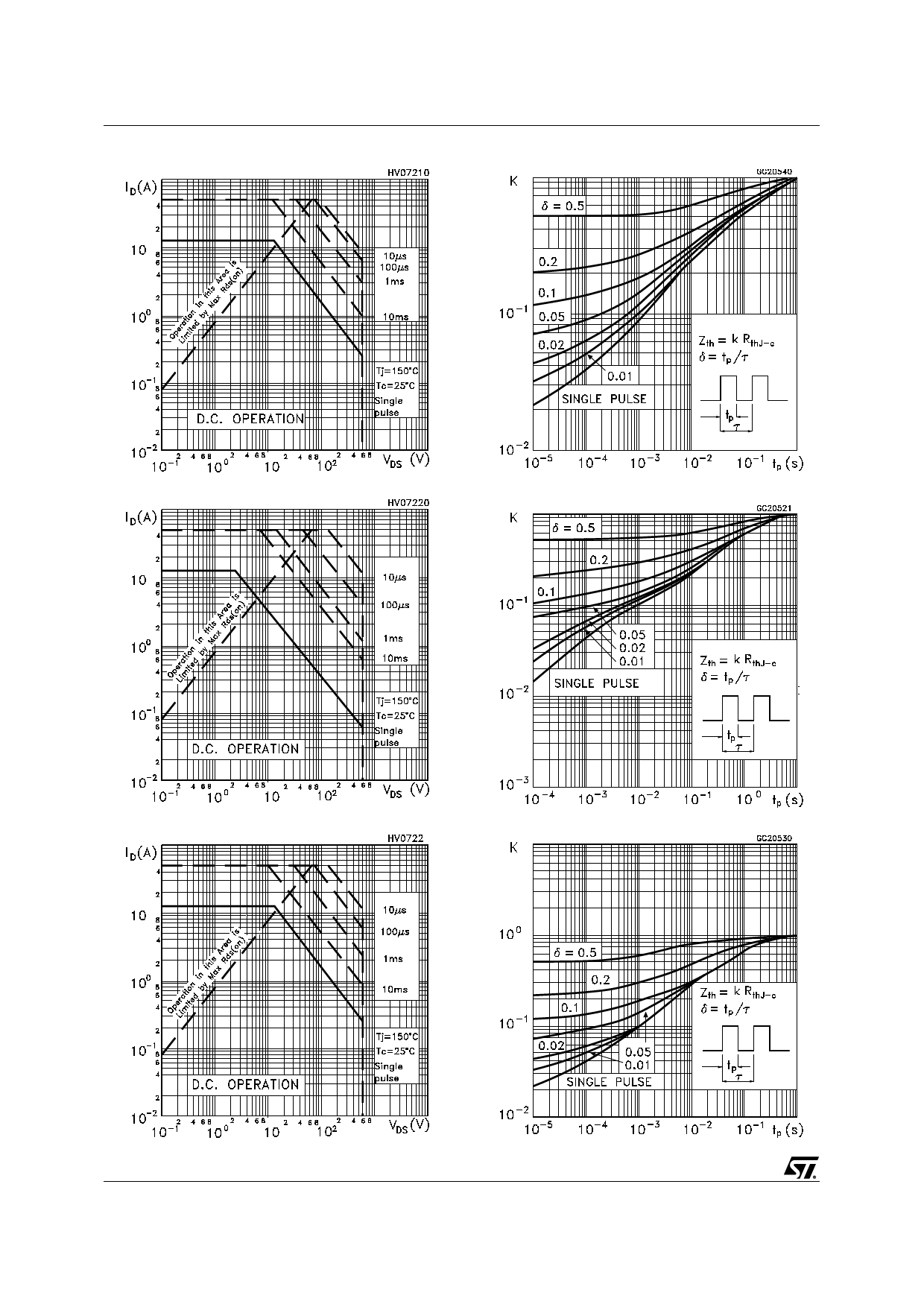
2 Electrical characteristics STB13NK60Z - STB13NK60Z-1 - STP13NK60Z/FP - STW13NK60Z
Table 7. Gate-source zener diode
Symbol
Parameter
Test Conditions
Min.
BVGSO
Note 6
Gate-Source Breakdown
Voltage
Igs=±1mA
(Open Drain)
30
Table 8. Source drain diode
Symbol
Parameter
Test Conditions
ISD
Source-drain Current
ISDMNote 2 Source-drain Current (pulsed)
VSDNote 4 Forward on Voltage
ISD = 10 A, VGS=0
trr
Qrr
IRRM
Reverse Recovery Time
Reverse Recovery Charge
Reverse Recovery Current
ISD= 10A, di/dt = 100A/µs,
VDD=35 V, Tj=150°C
Min.
Typ.
Max. Unit
V
Typ. Max. Unit
10
A
40
A
1.6
V
570
ns
4.5
µC
16
A
(1) Limited only by maximum temperature allowed
(2) Pulse width limited by safe operating area
(3) ISD ≤13A, di/dt ≤200A/µs, VDD ≤ V(BR)DSS, Tj ≤ TJMAX
(4) Pulsed: pulse duration = 300µs, duty cycle 1.5%
(5) Coss eq. is defined as a constant equivalent capacitance giving the same charging time as Coss when VDS increases from 0
to 80%
(6) The built-in back-to-back Zener diodes have specifically been designed to enhance not only the device’s ESD capability,
but also to make them safely absorb possible voltage transients that may occasionally be applied from gate to source. In
this respect the Zener voltage is appropriate to achieve an efficient and cost-effective intervention to protect the device’s
integrity. These integrated Zener diodes thus avoid the usage of external components.
(7) When mounted on minimum Footprint
4/17
Share Link: