CY23S08SI-2 查看數據表(PDF) - Cypress Semiconductor
零件编号
产品描述 (功能)
比赛名单
CY23S08SI-2 Datasheet PDF : 10 Pages
| |||
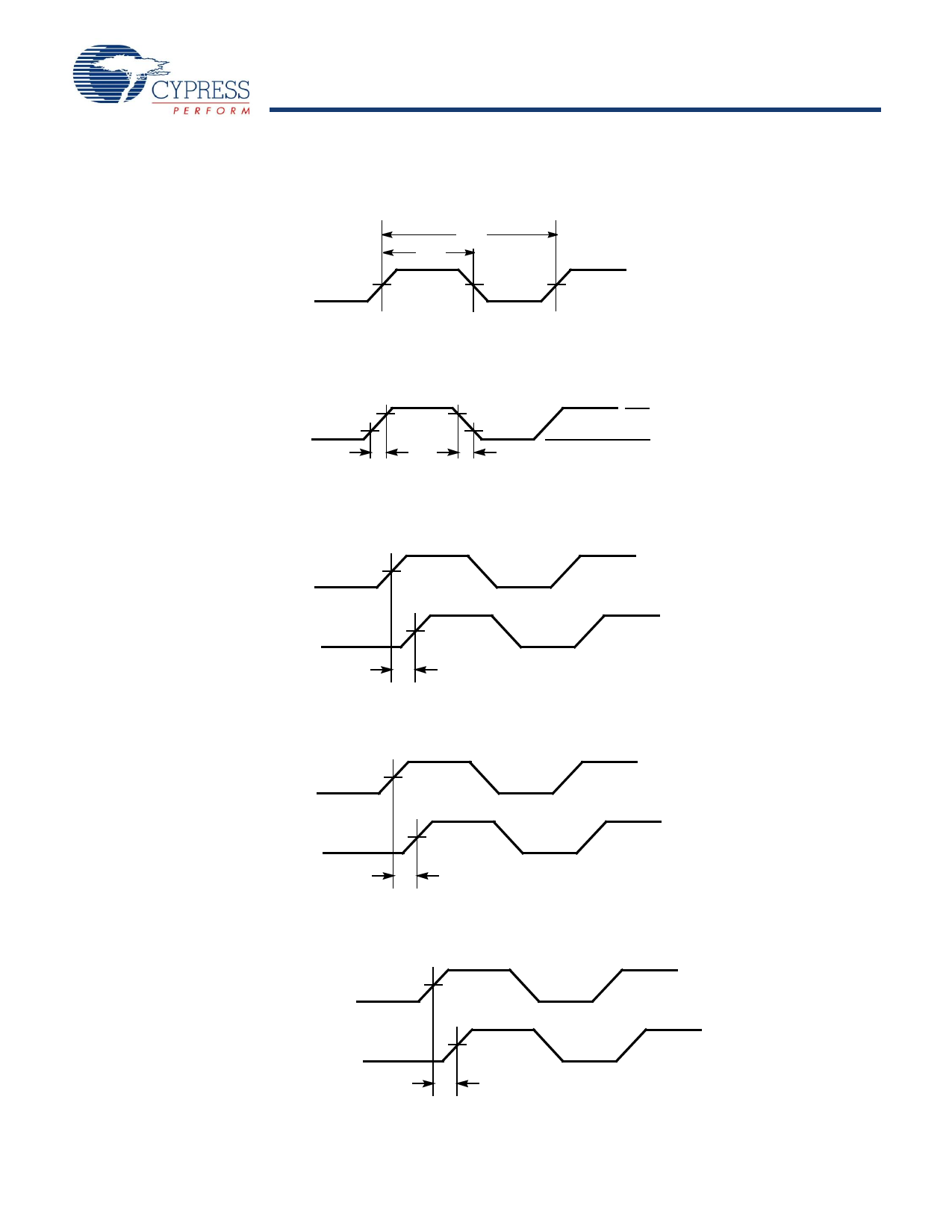
Switching Waveforms
Figure 2. Duty Cycle Timing
1.4V
t1
t2
1.4V
1.4V
Figure 3. All Outputs Rise and Fall Time
2.0V
OUTPUT 0.8V
t3
2.0V
0.8V
t4
3.3V
0V
Figure 4. Output-Output Skew
OUTPUT
1.4V
OUTPUT
t5
1.4V
Figure 5. Input-Output Propagation Delay
INPUT
VDD/2
FBK
t6
VDD/2
Figure 6. Device-Device Skew
FBK, Device 1
VDD/2
FBK, Device 2
t7
VDD/2
Document #: 38-07265 Rev. *H
CY23S08
Page 6 of 10
[+] Feedback
Share Link: 