LC86E7148 查看數據表(PDF) - SANYO -> Panasonic
零件编号
产品描述 (功能)
比赛名单
LC86E7148 Datasheet PDF : 20 Pages
| |||
LC86E7148
Parameter
LCD output
regulation
Symbol
Pins
VODLS S0 to S13,
S16 to S31
VODLC COM0 to COM3
LCD ladder
resistor
RLCD(1)
RLCD(2)
Pull-up MOS Rpu
Tr. resistor
Hysteresis
voltage
VHIS
Pin capacitance CP
•Ports 0, 1
•Ports A, B, C, D
•Ports 70, 71, 72, 73
•Ports 0, 1
•Ports 70, 71, 72, 73
• RES
All pins
Conditions
Ratings
VDD[V] min.
typ.
•Deference voltage
to ideal value
•VLCD, 2/3VLCD,
1/3VLCD
4.5-6.0 0
•Deference voltage
4.5-6.0 0
to ideal value
•VLCD, 2/3VLCD,
1/2VLCD, 1/3VLCD
Resistance at a
4.5-6.0
60
ladder resistor
•Resistance at a
4.5-6.0
30
ladder resistor
•1/2R mode
VOH=0.9VDD
4.5-6.0 15
40
max. unit
±0.2 V
±0.2
kΩ
70
Output disable
4.5-6.0
0.1VDD
V
•f=1MHz
•Unmeasurement
terminals for the
input are set to
VSS level.
•Ta=25°C
4.5-6.0
10
pF
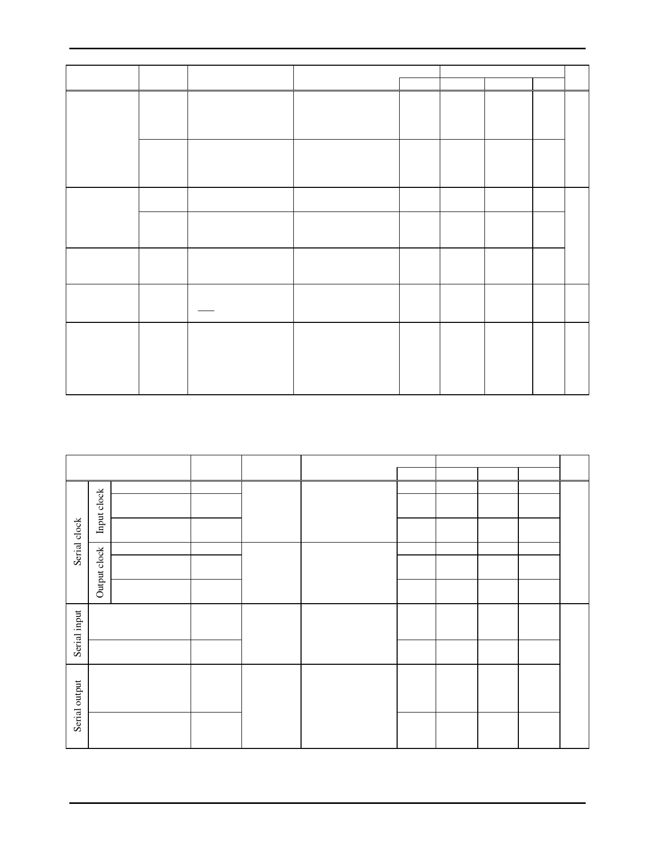
4. Serial Input / Output Characteristics at Ta=+10°C to +40°C, VSS=VSS1=VSS2=VSS3=0V
Parameter
Cycle
Low Level
pulse width
High Level
pulse width
Cycle
Low Level
pulse width
High Level
pulse width
Data set up time
Data hold time
Output delay time
(Serial clock is
external clock)
Output delay time
(Serial clock is
internal clock)
Symbol
Pins
tCKCY(1) SCK0,
tCKL(1) SCK1
Conditions
Refer to figure 5.
tCKH(1)
tCKCY(2) SCK0,
tCKL(2) SCK1
tCKH(2)
tICK
•SI0,SI1
•SB0,SB1
tCKI
tCKO(1) •SO0, SO1
•SB0, SB1
tCKO(2)
•Use pull-up
resistor (1kΩ)
when open drain
output.
•Refer to figure 5.
•Data set-up to
SCK0, 1
•Data hold from
SCK0, 1
•Refer to figure 5.
•Use pull-up
resistor (1kΩ)
when open drain
output.
•Data hold from
SCK0, 1
•Refer to figure 5.
VDD[V] min.
4.5-6.0 2
4.5-6.0 1
Ratings
typ.
max. unit
tCYC
4.5-6.0 1
4.5-6.0 2
4.5-6.0
1/2
tCKCY
4.5-6.0
1/2
tCKCY
4.5-6.0 0.1
µs
4.5-6.0 0.1
4.5-6.0
7/12tCYC
+0.2
4.5-6.0
1/3tCYC
+0.2
No.6748-13/20
Share Link: 