LC86E7148 查看數據表(PDF) - SANYO -> Panasonic
零件编号
产品描述 (功能)
比赛名单
LC86E7148 Datasheet PDF : 20 Pages
| |||
LC86E7148
Pin name I/O
Function description
PORT A
I/O • Segment output terminal for LCD display
-
(S0/PA0 –
• Can be used as a general input/output port
S7/PA7)
PORT B
I/O • Segment output terminal for LCD display
-
(S8/PB0 –
• Can be used as a general input/output port
S13/PB5)
PORT C
I/O • Segment output terminal for LCD display
-
(S16/PC0 –
• Can be used as a general input/output port
S23/PC7)
Option
PORT D
I/O • Segment output terminal for LCD display
-
(S24/PD0 –
• Can be used as a general input/output port
S31/PD7)
PORT L
I/O • Common output terminal for LCD display
-
(COM0/PL0 –
• Can be used as a general input port
COM3/PL3)
V1/PL4 –
I • Bias power terminal for LCD drive
-
V3/PL6
• Can be used as a general input port
RES
I Reset pin
-
XT1/ P74
I • Input pin for 32.768kHz crystal oscillation
-
In case of non use, connect to VDD.
• Other function
A general input port P74
XT2/P75
O • Output pin for 32.768kHz crystal oscillation -
In case of non use, should be left unconnected
( I ) • Other function
A general input port P75
CF1
I Input pin for ceramic resonator oscillation
-
CF2
O Output pin for ceramic resonator oscillation
-
* All of port options can be specified in bit unit except the pull-up resistor of port 0.
[Notes] • The VDD1, VDD2 and VDD3 terminals must be shorted electrically each other.
• The VSS1, VSS2 and VSS3 terminals must be shorted electrically each other.
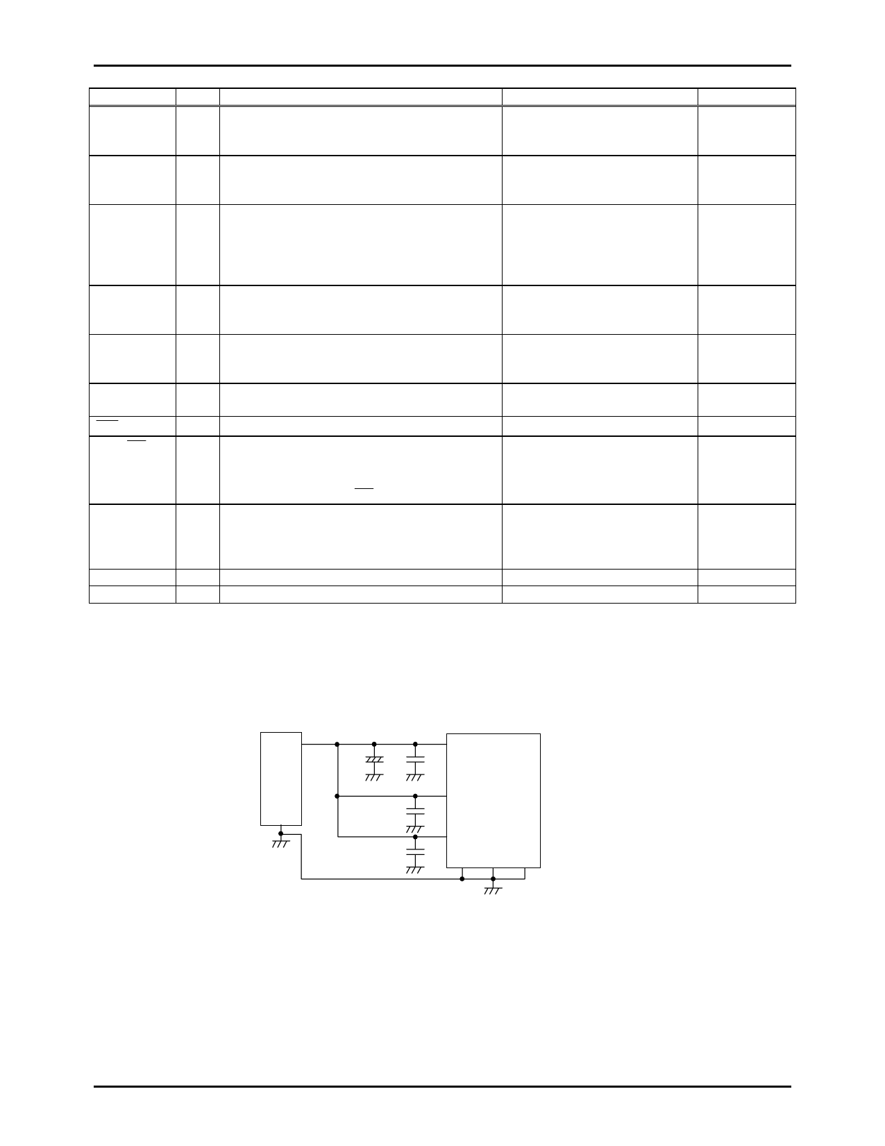
*1 Connect like the following figure to reduce noise into a VDD terminals.
Power
Supply
LSI
VDD1
VDD2
VDD3
VSS1 VSaS2 VSS3
*2 Memory select input for data security
*3 Output enable input
*4 Chip enable input
*5 TA ! PROM control signal input
PROM mode
Address input
A0 to A7
Address input
A8 to A13
PROM control
signal input
•TA(*5)
Address input
•A14,A15
No.6748-8/20
Share Link: 