LV8405V 查看數據表(PDF) - SANYO -> Panasonic
零件编号
产品描述 (功能)
比赛名单
LV8405V Datasheet PDF : 6 Pages
| |||
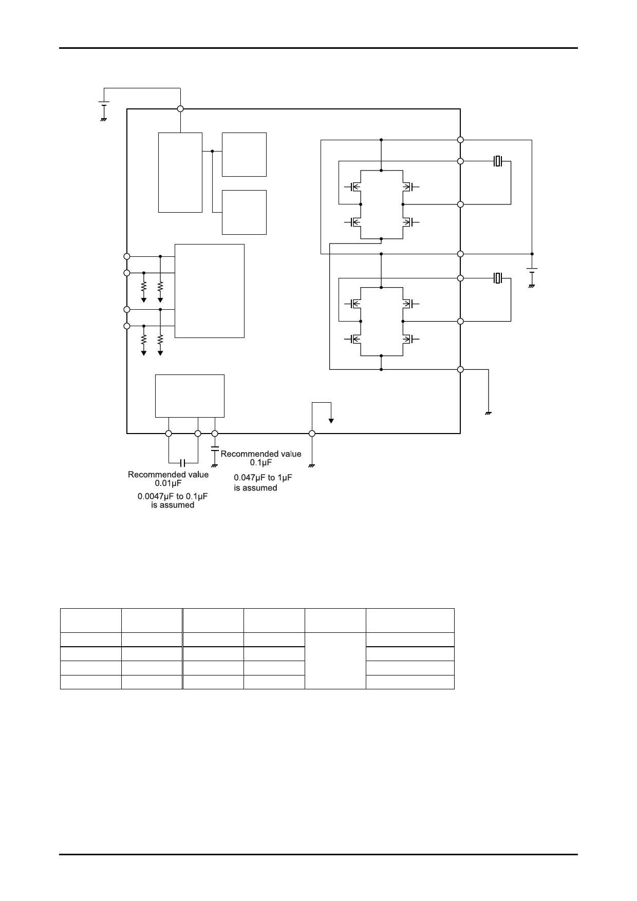
Block Diagram
LV8405V
Control voltage
2.8V to 5.5V
IN1
IN2
IN3
IN4
VCC
Startup
control
block
Thermal
Protection
Circuit
Reduced-
voltage
protection
circuit
Motor control
logic
Charge pump
VCC+VM
C1H C1L
VG
SGND
VM
OUT1
OUT2
VM
OUT3
OUT4
Motor power
supply
1.5V to 15V
PGND
* Connect a kickback absorption capacitor as near as possible to the IC. Coil kickback may cause increase in VM line
voltage, and a voltage exceeding the maximum rating may be applied momentarily to the IC, which results in
deterioration or damage of the IC
Truth Table
IN1
(IN3)
H
IN2
(IN4)
H
H
L
L
H
L
L
OUT1
(OUT3)
Z
L
H
L
OUT2
(OUT4)
Z
Charge pump
ON
Mode
Standby
H
Reverse
L
Forward
L
Brake
- : denotes a don't care value. Z : High-impedance
• The charge pump is always activated as long as VCC is applied.
* All power transistors turn off and the motor stops driving when the IC is detected in low voltage or thermal protection
mode.
No.A1340-4/6
Share Link: 