LC86E4448 查看數據表(PDF) - SANYO -> Panasonic
零件编号
产品描述 (功能)
比赛名单
LC86E4448 Datasheet PDF : 20 Pages
| |||
LC86E4448
Parameter
Symbol
Pins
Input clamp
voltage
Pin capacitance
VCLMP
CP
CVIN
All pins
Conditions
Ratings
Unit
VDD [V]
min
typ max
5.0
2.3
2.5 2.7
V
• f = 1 MHz
4.5 to 5.5
10
pF
• Unmeasured
input pins
are set to
VSS level.
• Ta = 25°C
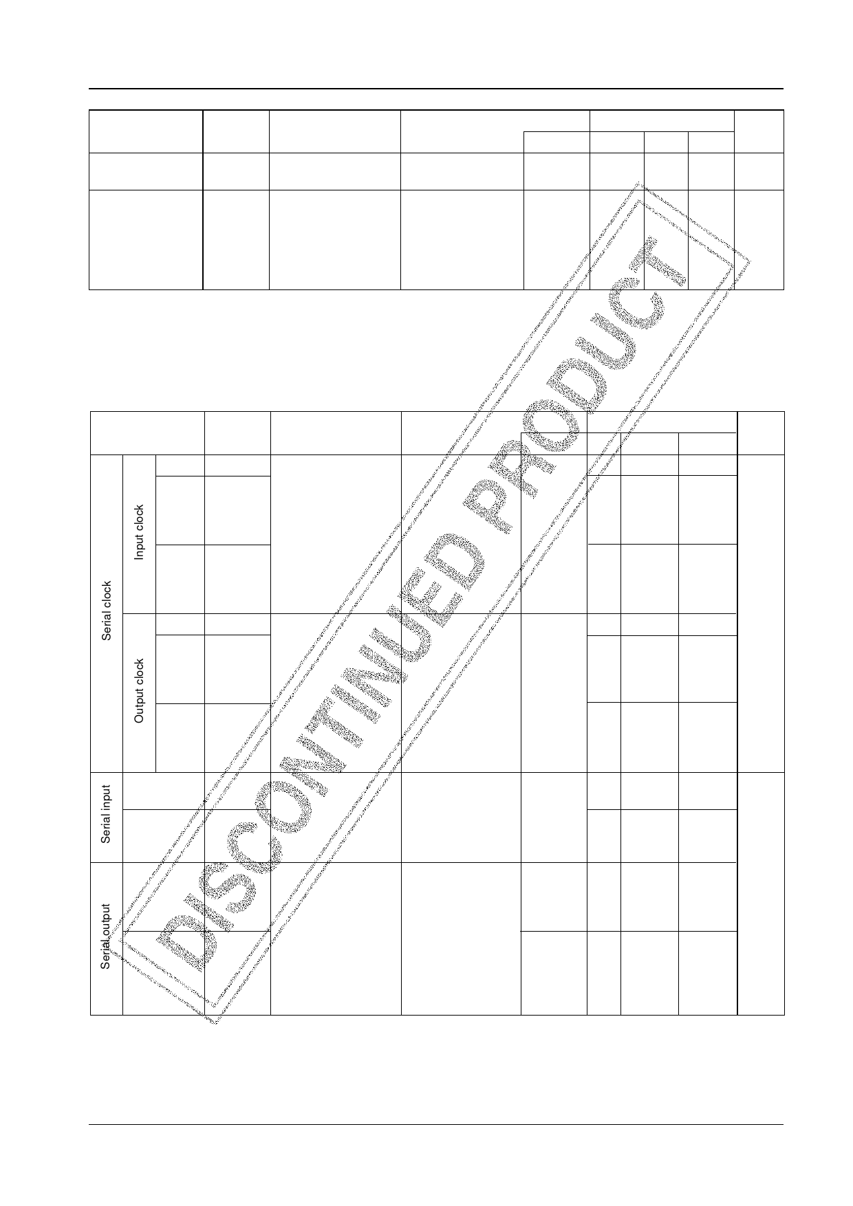
4. Serial Input/output Characteristics at Ta = +10°C to +40°C , VSS = 0 V
Parameter
Symbol
Pins
Cycle
Low-
level
pulse
width
High-
level
pulse
width
Cycle
Low-
level
pulse
width
High-
level
pulse
width
Data set-up
time
Data hold
time
tCKCY(1) • SCK0
tCKL(1) • SCLK0
tCKH(1)
tCKCY(2) • SCK0
tCKL(2) • SCLK0
tCKH(2)
tICK
SI0
tCKI
Output delay
time
(External
serial clock)
Output delay
time
(External
serial clock)
tCKO(1) SO0
tCKO(2)
Conditions
VDD [V] min
Refer to Figure 6.
4.5 to 5.5 2
1
Ratings
typ
max
Unit
tCYC
1
• Use a pull-up
resistor (1 kΩ)
when open drain
output
• Refer to Figure 6.
4.5 to 5.5
2
1/2tCKCY
1/2tCKCY
• Data set-up to
SCK0 rising
• Data hold from
SCK0 rising
• Refer to Figure 6.
• Use a pull-up
resistor (1 kΩ)
when open drain
output
• Data set-up to
SCK0 falling
• Data hold from
SCK0 falling
• Refer to Figure 6.
4.5 to 5.5 0.1
0.1
4.5 to 5.5
4.5 to 5.5
µs
7/12tCYC
+0.2
1/3tCYC
+0.2
No. 5648-13/20
Share Link: 