DMP3030SN 查看數據表(PDF) - ZP Semiconductor
零件编号
产品描述 (功能)
比赛名单
DMP3030SN Datasheet PDF : 1 Pages
| |||
DMP3030SN
Features
• Low On-Resistance
• Low Gate Threshold Voltage
• Low Input Capacitance
• Fast Switching Speed
• Lead Free By Design/RoHS Compliant (Note 2)
• ESD Protected Gate
• "Green" Device (Note 4)
• Qualified to AEC-Q101 standards for High Reliability
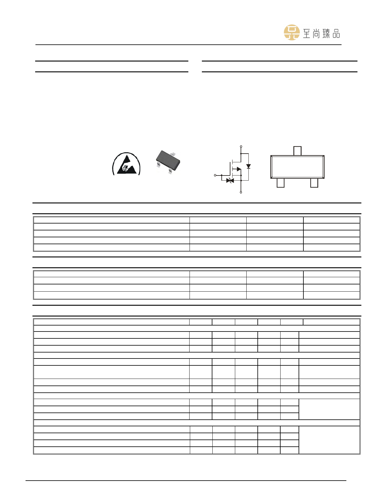
Mechanical Data
• Case: SC59
• Case Material: Molded Plastic, “Green” Molding
Compound. UL Flammability Classification Rating 94V-0
• Moisture sensitivity: Level 1 per J-STD-020C
• Terminals: Finish ⎯ Matte Tin annealed over Copper
leadframe. Solderable per MIL-STD-202, Method 208
• Terminal Connections: See Diagram
• Weight: 0.014 grams (approximate)
SC59
Drain
D
ESD protected
TOP VIEW
Maximum Ratings @TA = 25°C unless otherwise specified
Characteristic
Drain-Source Voltage
Gate-Source Voltage
Drain Current (Note 1) Steady State
Pulsed Drain Current (Note 3)
Gate
Gate
Protection
Diode
Source
EQUIVALENT CIRCUIT
G
S
Internal Schematic
Symbol
VDSS
VGSS
ID
IDM
Value
-30
±20
-0.7
-2.8
Unit
V
V
A
A
Thermal Characteristics @TA = 25°C unless otherwise specified
Characteristic
Total Power Dissipation (Note 1)
Thermal Resistance, Junction to Ambient
Operating and Storage Temperature Range
Symbol
Pd
RθJA
Tj, TSTG
Value
500
250
-65 to +150
Unit
mW
°C/W
°C
Electrical Characteristics @TA = 25°C unless otherwise specified
Characteristic
OFF CHARACTERISTICS (Note 5)
Drain-Source Breakdown Voltage
Zero Gate Voltage Drain Current
Gate-Body Leakage
ON CHARACTERISTICS (Note 5)
Gate Threshold Voltage
Static Drain-Source On-Resistance
Forward Transfer Admittance
Diode Forward Voltage (Note 5)
DYNAMIC CHARACTERISTICS
Input Capacitance
Output Capacitance
Reverse Transfer Capacitance
SWITCHING CHARACTERISTICS
Turn-On Delay Time
Turn-Off Delay Time
Turn-On Rise Time
Turn-Off Fall Time
Notes:
1. Device mounted on FR-4 PCB.
2. No purposefully added lead.
3. Pulse width ≤10μS, Duty Cycle ≤1%.
Symbol Min
BVDSS
-30
IDSS
⎯
IGSS
⎯
VGS(th)
RDS (ON)
|Yfs|
VSD
-1.0
⎯
⎯
⎯
Ciss
⎯
Coss
⎯
Crss
⎯
tD(ON)
⎯
tD(OFF)
⎯
tr
⎯
tf
⎯
Typ
⎯
⎯
⎯
⎯
0.20
0.35
1
-0.8
160
120
50
10
25
25
40
Max
⎯
-10
±10
-3.0
0.25
0.45
⎯
-1.1
⎯
⎯
⎯
⎯
⎯
⎯
⎯
Unit
Test Condition
V VGS = 0V, ID = -250µA
μA VDS = -30V, VGS = 0V
μA VGS = ±20V, VDS = 0V
V VDS = -10V, ID = -1.0mA
Ω VGS = -10V, ID = -0.4A
VGS = -4.5V, ID = -0.4A
S VDS = -10V, ID = -0.4A
V VGS = 0V, IS = -0.7A
pF
pF
VDS = -10V, VGS = 0V
f = 1.0MHz
pF
ns
ns VDD = -10V, ID = -0.4A,
ns VGS = -5.0V, RGEN = 50Ω
ns
sales@zpsemi.com
www.zpsemi.com
1 of 1
Share Link: 