MAX4075BLEUA 查看數據表(PDF) - Maxim Integrated
零件编号
产品描述 (功能)
比赛名单
MAX4075BLEUA Datasheet PDF : 20 Pages
| |||
Micropower, SOT23, Rail-to-Rail,
Fixed-Gain, GainAmp/Open-Loop Op Amps
GainAmp Bandwidth
GainAmp fixed-gain amplifiers feature factory-trimmed
precision resistors to provide fixed inverting gains from
-0.25V/V to -100V/V or noninverting gains from +1.25V/V
to +101V/V. The op amp core is decompensated strate-
gically over the gain-set options to maximize band-
width. Open-loop decompensation increases GBW
product, ensuring that usable bandwidth is maintained
with increasing closed-loop gains. A GainAmp with a
fixed gain of AV = +25V/V has a -3dB bandwidth of
120kHz. By comparison, a unity-gain-stable op amp con-
figured for AV = +25V/V would yield a -3dB bandwidth
of only 8kHz. Decompensation is performed at five inter-
mediate gain sets, as shown in the Gain Selector
Guide.
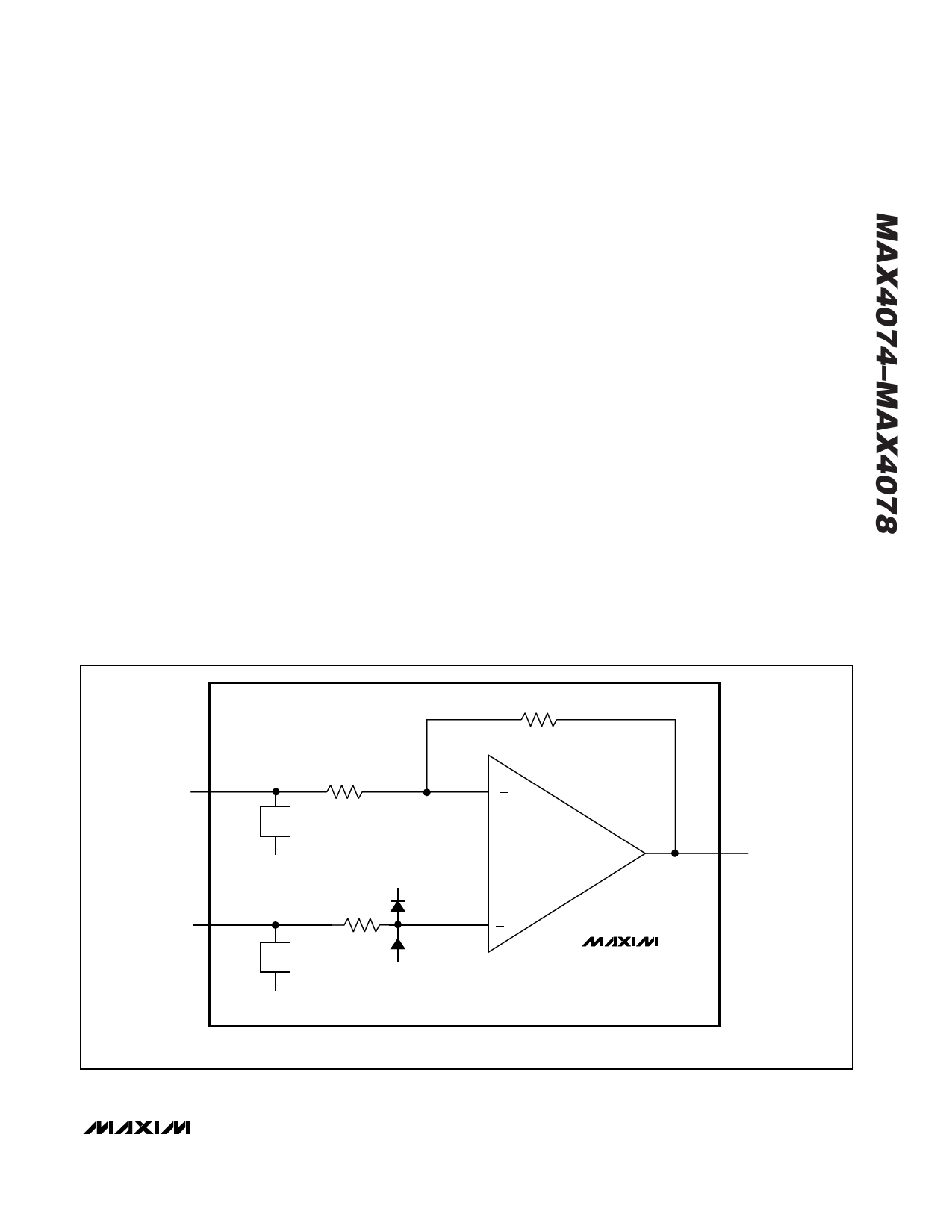
High-Voltage (±17V)
Input Fault Protection
The MAX4074/MAX4075 family includes ±17V input
fault protection. For normal operation, see the input
voltage range specification in the Electrical Character-
istics. Overdriven inputs up to ±17V will not cause out-
put phase reversal. A back-to-back SCR structure at
the input pins allows either input to safely swing ±17V
relative to VEE (Figure 2). Additionally, the internal op
amp inputs are diode clamped to both supply rails for
the protection of sensitive input stage circuitry. Current
through the clamp diodes is limited by a 5kΩ resistor at
the noninverting input, and by RG at the inverting input.
An IN+ or IN- fault voltage as high as ±17V causes less
than 3.5mA to flow through the input pin, protecting
both the GainAmp and the signal source from damage.
Applications Information
GainAmp fixed-gain amplifiers offer a precision, fixed-
gain amplifier in a small package that can be used in a
variety of circuit board designs. GainAmp fixed-gain
amplifiers can be used in many op amp circuits that
use resistive negative feedback to set gain, and do not
require other connections to the op amp inverting input.
Both inverting and noninverting op amp configurations
can be implemented easily using a GainAmp.
GainAmp Input Voltage Range
The MAX4074/MAX4075 combine both an op amp and
gain-setting feedback resistors on the same IC. The
inverting input voltage range is different from the nonin-
verting input voltage range because the inverting input
pin is connected to the RG input series resistor. Just as
with a discrete design, take care not to saturate the
inputs/output of the core op amp to avoid signal distor-
tions or clipping.
RF
IN-
RG
17V
SCR
OUT
VEE
VCC
IN+
5k
17V
SCR
VEE
VEE
MAX4074
MAX4075
Figure 2. Input Protection
NOTE: INPUT STAGE PROTECTION INCLUDES TWO 17V SCRs
AND TWO DIODES AT THE INPUT STAGE.
______________________________________________________________________________________ 11
Share Link: 