MAX4075AEEUA 查看數據表(PDF) - Maxim Integrated
零件编号
产品描述 (功能)
比赛名单
MAX4075AEEUA Datasheet PDF : 20 Pages
| |||
Micropower, SOT23, Rail-to-Rail,
Fixed-Gain, GainAmp/Open-Loop Op Amps
ABSOLUTE MAXIMUM RATINGS
Supply Voltages (VCC to VEE) ..................................-0.3V to +6V
Voltage Inputs (IN_)
MAX4076/MAX4077/MAX4078 .....(VCC + 0.3V) to (VEE - 0.3V)
MAX4074/MAX4075 ..........................................................±17V
Output Short-Circuit Duration to Either Supply (OUT_)....Continuous
Continuous Power Dissipation (TA = +70°C)
5-Pin SOT23 (derate 7.1mW/°C above +70°C) ............571mW
14-Pin TSSOP (derate 6.3mW/°C above +70°C) ..........500mW
8-Pin µMAX (derate 4.1mW/°C above +70°C) ..............330mW
8-Pin SO (derate 5.88mW/°C above +70°C).................471mW
14-Pin SO (derate 8.33mW/°C above +70°C)...............667mW
Operating Temperature Range ...........................-40°C to +85°C
Junction Temperature ......................................................+150°C
Storage Temperature Range .............................-65°C to +150°C
Lead Temperature (soldering, 10sec) .............................+300°C
Stresses beyond those listed under “Absolute Maximum Ratings” may cause permanent damage to the device. These are stress ratings only, and functional
operation of the device at these or any other conditions beyond those indicated in the operational sections of the specifications is not implied. Exposure to
absolute maximum rating conditions for extended periods may affect device reliability.
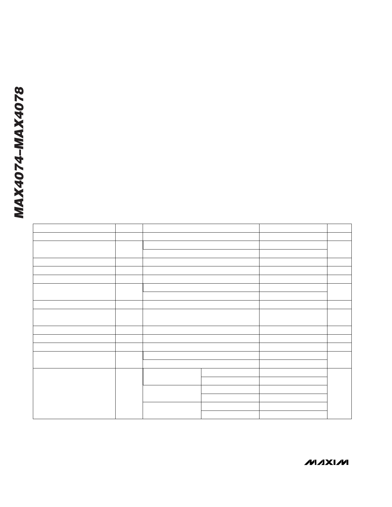
ELECTRICAL CHARACTERISTICS—MAX4074/MAX4075
(VCC = +2.5V to +5.5V, VEE = 0, VIN+ = VIN- = VCC/2, RL = ∞ to VCC/2, TA = TMIN to TMAX, unless otherwise noted. Typical values
are at VCC = +5V and TA = +25°C.) (Note 1)
PARAMETER
Supply Voltage Range
Supply Current (per amplifier)
Input Offset Voltage
Input Offset Voltage Drift
Input Bias Current (Note 2)
Inverting Input Resistance
Noninverting Input Resistance
SYMBOL
VCC
ICC
VOS
CONDITIONS
Guaranteed by PSRR test
VCC = 5V
VCC = 3V
RL = 1MΩ
IIN+_
RIN_
RIN_+
AV < +25V/V
AV ≥ +25V/V
Positive Input Voltage Range
IN_+ Guaranteed by functional test (Note 3)
Negative Input Voltage Range
Power-Supply Rejection Ratio
Closed-Loop Output Impedance
IN_-
PSRR
ROUT
Output Short-Circuit Current
Output Voltage Swing (Note 4)
Guaranteed by functional test (Note 3)
VCC = 2.5V to 5.5V
Shorted to VCC
Shorted to VEE
RL = 1MΩ
RL = 10kΩ
RL = 1kΩ
VCC - VOH
VOL - VEE
VCC - VOH
VOL - VEE
VCC - VOH
VOL - VEE
MIN
2.5
VEE -
0.15
70
TYP
37
34
0.2
0.3
0.8
300
80
1000
±15
96
0.2
5
-22
0.5
0.4
25
11
300
100
MAX
5.5
55
50
3.5
1000
UNITS
V
µA
mV
µV/°C
pA
kΩ
MΩ
VCC -
1.2
V
V
dB
Ω
mA
2.5
2.5
150
mV
80
1000
600
2 _______________________________________________________________________________________
Share Link: 