LT8302HS8E-3-WPBF 查看數據表(PDF) - Analog Devices
零件编号
产品描述 (功能)
比赛名单
LT8302HS8E-3-WPBF
Analog Devices

LT8302HS8E-3-WPBF Datasheet PDF : 26 Pages
| |||
LT8302/LT8302-3
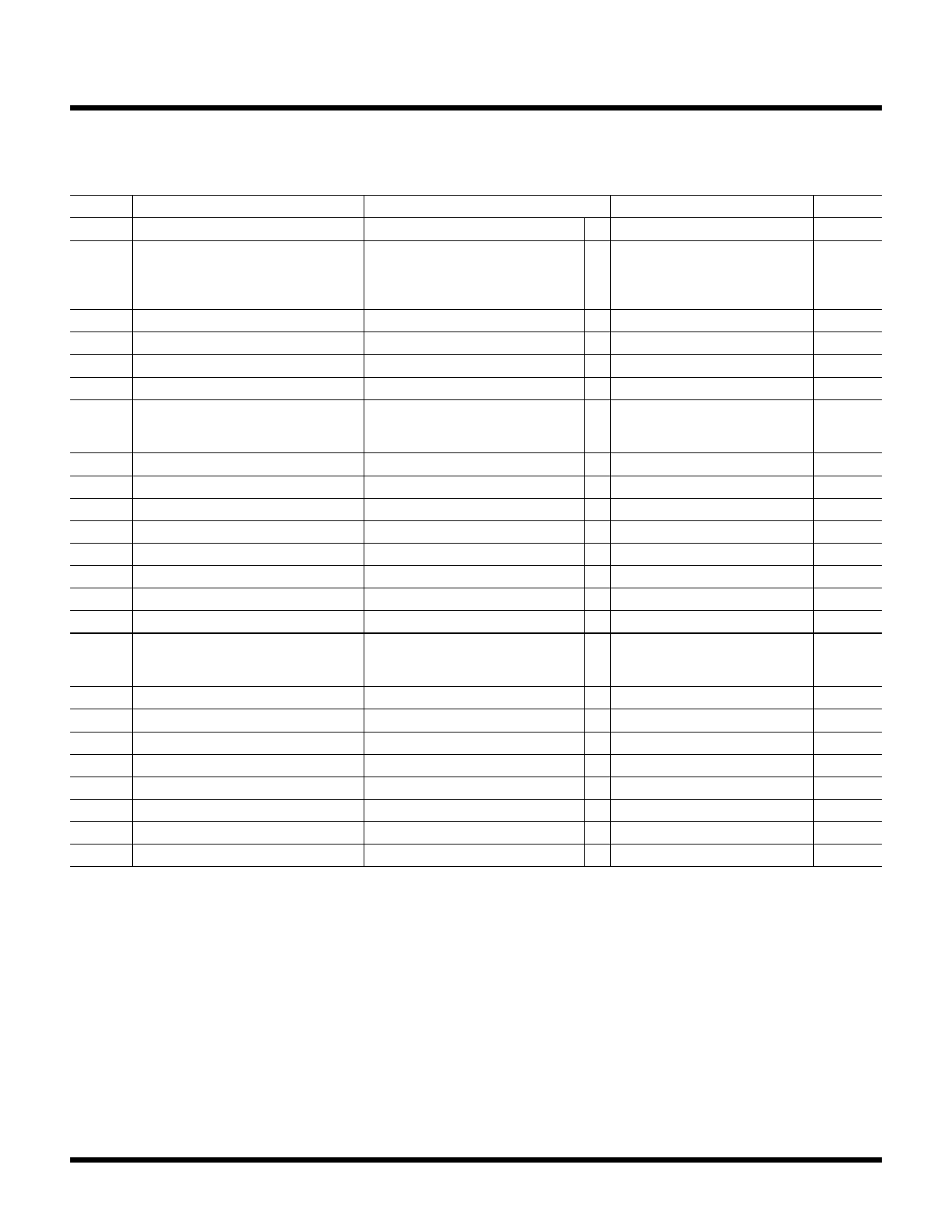
ELECTRICAL CHARACTERISTICS The l denotes the specifications which apply over the full operating
temperature range, otherwise specifications are at TA = 25°C. VIN = 5V, VEN/UVLO = VIN, CINTVCC = 1µF to GND, unless otherwise noted.
SYMBOL
VIN
IQ
IHYS
VINTVCC
IINTVCC
VTC
ITC
fMIN
tON(MIN)
tOFF(MAX)
ISW(MAX)
ISW(MIN)
RDS(ON)
ILKG
tSS
PARAMETER
VIN Voltage Range
VIN Quiescent Current
EN/UVLO Shutdown Threshold
EN/UVLO Enable Threshold
EN/UVLO Enable Threshold
EN/UVLO Enable Hysteresis
EN/UVLO Hysteresis Current
INTVCC Regulation Voltage
INTVCC Current Limit
INTVCC UVLO Threshold
INTVCC UVLO Hysteresis
(RFB – VIN) Voltage
RREF Regulation Voltage
RREF Regulation Voltage Line Regulation
TC Pin Voltage
TC Pin Current
Minimum Switching Frequency
Minimum Switch-On Time
Maximum Switch-Off Time
Maximum Switch Current Limit
Minimum Switch Current Limit
Switch On-Resistance
Switch Leakage Current
Soft-Start Timer
CONDITIONS
VEN/UVLO = 0.2V
VEN/UVLO = 1.1V
Sleep Mode (Switch Off)
Active Mode (Switch On)
For Lowest Off IQ
Falling (E, I, H, MP Grades)
Falling (J Grade Only)
VEN/UVLO = 0.3V
VEN/UVLO = 1.1V
VEN/UVLO = 1.3V
IINTVCC = 0mA to 10mA
VINTVCC = 2.8V
Falling
IRFB = 75µA to 125µA
3V ≤ VIN ≤ 42V
VTC = 1.2V (LT8302)
VTC = 1.2V (LT8302-3)
VTC = 0.8V
Backup Timer
ISW = 1.5A
VSW = 65V
MIN
TYP
MAX
UNIT
l
3
42
V
0.5
2
µA
53
µA
106
µA
380
µA
l 0.2
0.75
V
l 1.178
1.214
1.250
V
l 1.160
1.214
1.268
V
14
mV
–0.1
0
0.1
µA
2.3
2.5
2.7
µA
–0.1
0
0.1
µA
2.85
3
3.1
V
10
13
20
mA
2.39
2.47
2.55
V
105
mV
–50
50
mV
l 0.98
1.00
1.02
V
–0.01
0
0.01
%/V
1.00
V
12
15
18
µA
7
10
13
µA
–200
µA
11.3
12
12.7
kHz
160
ns
170
µs
3.6
4.5
5.4
A
0.70
0.87
1.04
A
80
mΩ
0.1
0.5
µA
11
ms
Note 1: Stresses beyond those listed under Absolute Maximum Ratings
may cause permanent damage to the device. Exposure to any Absolute
Maximum Rating condition for extended periods may affect device
reliability and lifetime.
Note 2: The SW pin is rated to 65V for transients. Depending on the
leakage inductance voltage spike, operating waveforms of the SW pin
should be derated to keep the flyback voltage spike below 65V as shown
in Figure 5.
Note 3: The LT8302E/LT8302E-3 is guaranteed to meet performance
specifications from 0°C to 125°C junction temperature. Specifications
over the –40°C to 125°C operating junction temperature range are
assured by design, characterization and correlation with statistical process
controls. The LT8302I/LT8302I-3 is guaranteed over the full –40°C to
125°C operating junction temperature range. The LT8302J/LT8302J-3
and LT8302H/LT8302H-3 are guaranteed over the full –40°C to 150°C
operating junction temperature range. The LT8302MP is guaranteed
over the full –55°C to 150°C operating junction temperature range. High
junction temperatures degrade operating lifetimes. Operating lifetime is
derated at junction temperature greater than 125°C.
Note 4: The LT8302/LT8302-3 includes overtemperature protection that
is intended to protect the devices during momentary overload conditions.
Junction temperature will exceed 150°C when overtemperature protection
is active. Continuous operation above the specified maximum operating
junction temperature may impair device reliability.
Rev. G
For more information www.analog.com
3
Share Link: