IS62LV12816ALL-70B 查看數據表(PDF) - Integrated Silicon Solution
零件编号
产品描述 (功能)
比赛名单
IS62LV12816ALL-70B Datasheet PDF : 10 Pages
| |||
IS62LV12816ALL
AC TEST CONDITIONS
Parameter
Input Pulse Level
Input Rise and Fall Times
Input and Output Timing
and Reference Level
Output Load
Unit
0.4V to 2.2V
5 ns
1.3V
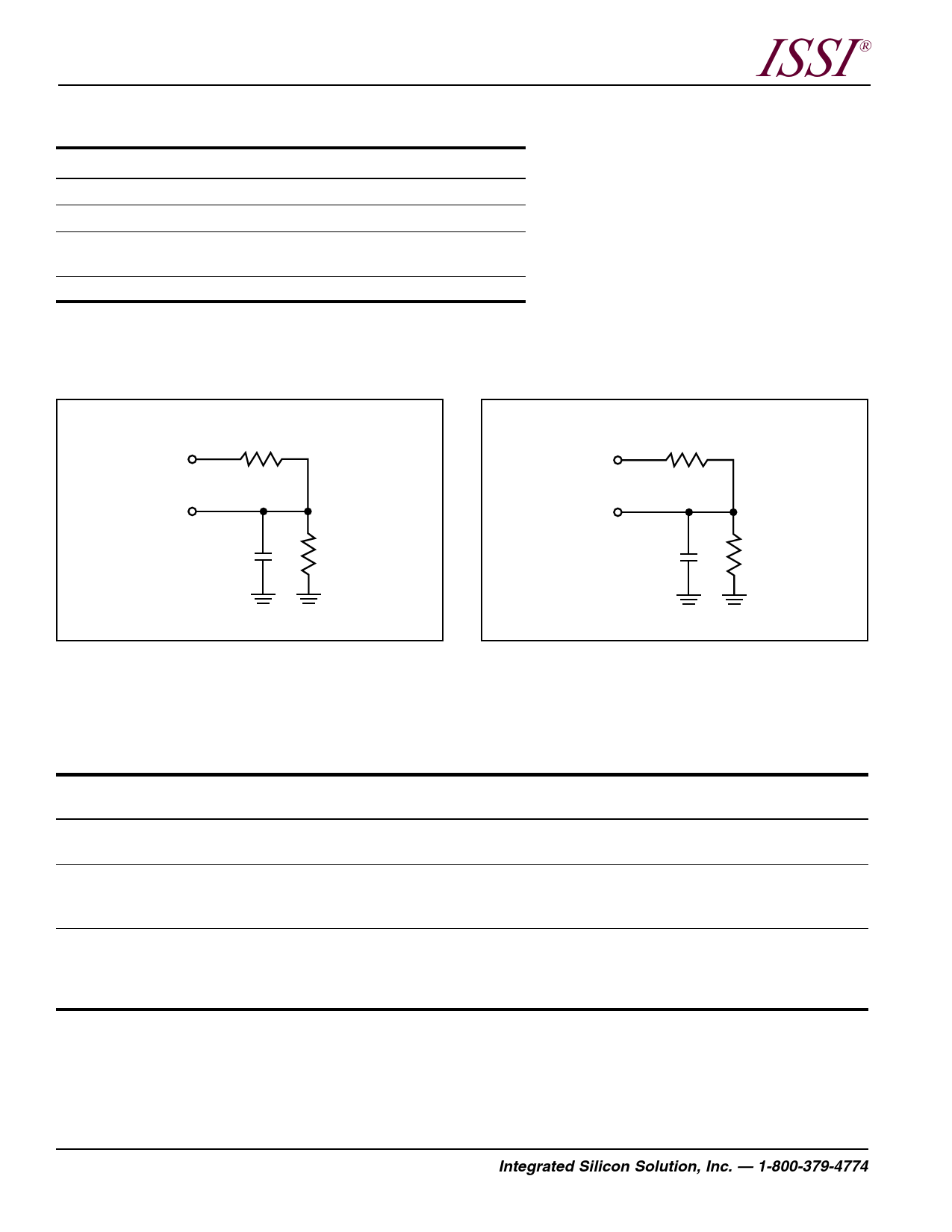
See Figures 1 and 2
ISSI ®
AC TEST LOADS
3.0V
3070 Ω
OUTPUT
100 pF
Including
jig and
scope
3150 Ω
Figure 1
3.0V
3070 Ω
OUTPUT
5 pF
Including
jig and
scope
3150 Ω
Figure 2
POWER SUPPLY CHARACTERISTICS(1) (Over Operating Range)
Symbol Parameter
Test Conditions
-55
-70
-100
Min. Max. Min. Max. Min. Max. Unit
ICC
Vcc Dynamic Operating VCC = Max.,
Com.
Supply Current
IOUT = 0 mA, f = fMAX
Ind.
— 40
— 60
— 30
— 50
— 20
mA
— 40
ISB1
TTL Standby Current VCC = Max.,
(TTL Inputs)
VIN = VIH or VIL
CE ≥ VIH , f = 0
Com.
Ind.
— 0.4
— 1.0
— 0.4
— 1.0
— 0.4 mA
— 1.0
ISB2
CMOS Standby
VCC = Max.,
Com.
Current (CMOS Inputs) CE ≥ VCC – 0.2V,
Ind.
VIN ≥ VCC – 0.2V, or
VIN ≤ 0.2V, f = 0
—5
—5
—5
µA
—5
—5
—5
Note:
1. At f = fMAX, address and data inputs are cycling at the maximum frequency, f = 0 means no input lines change.
4
Integrated Silicon Solution, Inc. — 1-800-379-4774
Rev. A
04/17/01
Share Link: 