RF133 查看數據表(PDF) - Conexant Systems
零件编号
产品描述 (功能)
比赛名单
RF133 Datasheet PDF : 17 Pages
| |||
RF133
RF/IF Transceiver
RF210
LNA/Image Reject Mixer
GSM
Rx Filter
IF SAW
Filter
DCS
Rx Filter
Tx/Rx VCO
DUAL PLL
UHF VCO
LC
Tank
RF133
PGA PGB
PGC
90˚
÷2 ÷4
÷2 ÷4
÷2 ÷4
PGD
DC
OC
PGD
Bias
3 Wire
Control
RXI
CTH1
T/H
CTH2
RXQ
SX ENA
RX ENA
TX ENA
DATA
CLK
LE
Antenna
Combiner
Tx/Rx VCO
÷1 ÷2
CHP
P F D ÷1 ÷2
LPF
TXI
90˚
T/R
Coupler
VAPC
Diplexer
RF142
T/R
RM008
TX DCS VCO
LOOP FILTER
TX GSM VCO
TX IF FILTER
LPF
TXQ
C453
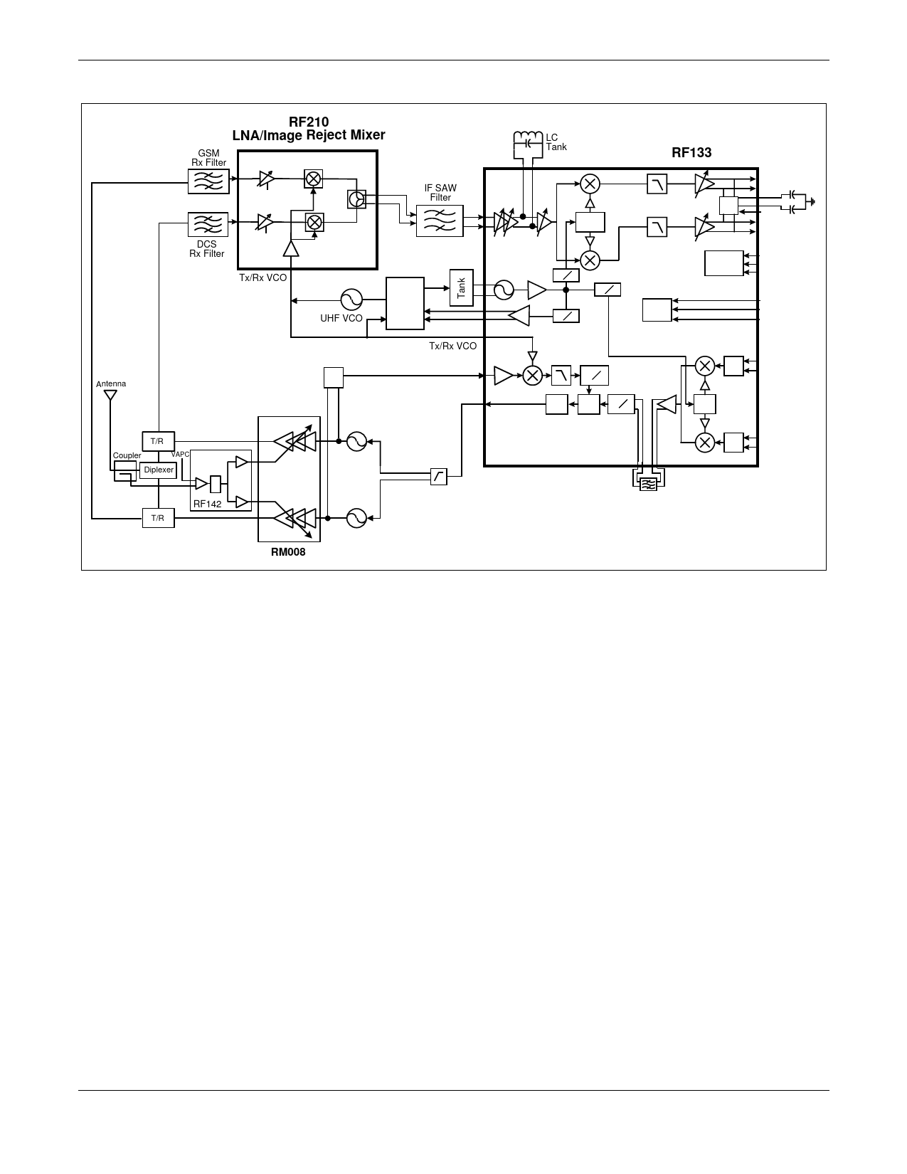
Figure 3. Dual-Band Transceiver Chipset Using The RF133
PGA has two gain settings, either 0 dB or 20 dB, whereas both
PGB and PGC have a gain range of -10 dB to 20 dB
programmable in 2 dB steps. The output of PGC is fed to a
quadrature mixer. The quadrature mixer has a fixed conversion
gain of 10 dB and its LO inputs are taken from the outputs of a
quadrature divider (divide by 2 or 4).
Baseband Integrated Filters, Baseband Amplifiers, and DC
Offset Compensation. Immediately following the quadrature
mixer (demodulator) is the baseband section (DC offset
compensation circuitry, two integrated baseband filters and two
programmable gain amplifiers). Each programmable gain
amplifier in the baseband section, both labelled PGD, has four
different gain settings: 0 dB, 10 dB, 20 dB, or 30 dB.
The corner frequency of the integrated baseband filters is
adjustable by using an appropriate value resistor at pin 26,
LPFADJ. At the nominal cutoff frequency of 105 kHz, the
resistor value is 75.1 kΩ.
Due to possible high gain of the baseband amplifiers (PGD), any
DC offsets at the outputs of the quadrature mixer are amplified
and, if uncorrected, the I and Q outputs can suffer from
significant unwanted DC offset voltages. To cancel out these
effects, the RF133 must be calibrated.
During compensation, the correction voltages are stored in
external hold capacitors CTH1 and CTH2, then the loop is
opened immediately thereafter. The corrected I and Q outputs
are then fed directly to external circuitry for further baseband
processing.
The timing diagram for this calibration sequence in reference to
the receive slot is shown in Figure 4 (the front-end mixer is
assumed to be Rockwell’s RF210 dual-band, image reject
downconverter). At first, the RF133 receiver is turned on
(RXENA is high). After time T1, the track and hold signal, T/H,
places the DC compensation circuitry in the track mode for time
T2. Then, there is a settling time, T3, before the external front-
end is turned on. Finally, the front-end must be turned on for
time T4 before the receive slot.
Time T2 can vary from 10 µsec to 350 µsec. This duration is
dependent on 1) the value of the hold capacitors (CTH1 and
CTH2), and 2) whether the calibration is done from frame to
frame or from a cold start. This is tabulated in Table 2.
4
October 8, 1999
Conexant
Proprietary Information and Specifications are Subject to Change
100776A
Share Link: 