G525A 查看數據表(PDF) - Global Mixed-mode Technology Inc
零件编号
产品描述 (功能)
比赛名单
G525A Datasheet PDF : 8 Pages
| |||
Global Mixed-mode Technology Inc.
G525A
Absolute Maximum Ratings
Supply Voltage (VIN)..…………….….………...…..+6.0V
Fault Flag Voltage (VFLG)..…………..……...……..+6.0V
Fault Flag Current (IFLG)……………………………50mA
Output Voltage (VOUT)..…………………………….+6.0V
Output Current (IOUT).………………….Internally Limited
Enable Input (VEN)……………………………-0.3V to 6V
Storage Temperature (TS)….………....-65°C to +150°C
Lead Temperature (Soldering 5 sec.)……………260°C
ESD protection*………………..…………….……….2kV
Operating Ratings
Supply Voltage (VIN).……………………….+3V to +5.5V
Operating Temperature (TA)…………….-40°C to +85°C
Thermal Resistance
SOIC (θJA)……………………………………160°C/W
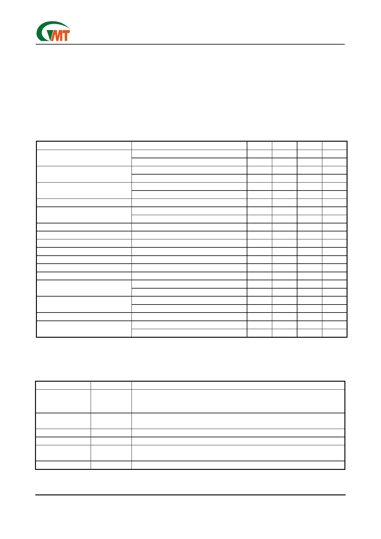
Electrical Characteristics (VIN=+5V; TA=25°C.)
PARAMETER
CONDITION
MIN TYP MAX UNITS
IN Supply Current
**switch off, OUT = open
**switch on, OUT = open
1
5
µA
100
160
µA
EN Enable Threshold
low to high transition
high to low transition **
2.5
V
0.8
V
EN Input Current
EN Input Capacitance
VEN = VOH(min) = 2.5V
VEN = VOL(max) = 1.0V
0.01
1
µA
0.01
1
µA
1
pF
Switch Resistance
OUT Turn-On Delay
OUT Turn-On Rise Time
OUT Turn-Off Delay
OUT Turn-Off Fall Time
OUT Leakage Current
VIN = 5V , IOUT = 500mA
VIN = 3.3V , IOUT = 500mA
RL = 10Ω
RL = 10Ω, CL=100µF
RL = 10Ω
RL = 10Ω
110
140
mΩ
130
180
mΩ
0.03
ms
0.5
ms
1
20
µs
1
20
µs
1
10
µA
Short Circuit Current Limit
Enable into load
1.0
1.4
2.0
A
Circuit Limit Threshold
Ramped load applied to enabled output
2.0
2.7
3.5
A
Overtemperature Shutdown
TJ increasing
135
°C
Threshold
TJ decreasing
125
°C
FLG Output Resistance
VIN = 5V, IL=10mA
VIN = 3.3V, IL =10mA
10
25
Ω
15
40
Ω
FLG Off Current
VFLAG = 5V
0.01
1
µA
UVLO Threshold
VIN = increasing
VIN = decreasing
2.5
V
2.3
V
* Devices are ESD protected, however, handling precautions are recommended.
** For the G525A1, off is ≤ 1.0 and on is ≥2.5V. For the G525A2, off is ≥ 2.5V and on is ≤ 1.0V. The enable input,
CTRL, has approximately 200mV of hysteresis.
Pin Description
PIN NUMBER
1
2
3
4,5
7
6,8
PIN NAME
EN
FLG
GND
NC
IN
OUT
PIN FUNCTION
Enable (input): Logic level enable input. High input >2.4V typical.
Low input <2.2V typical (1 for active high, 2 for active low).
Make sure EN never floating.
Open-Drain Fault Flag (Output): Active-low, open-drain output. Indicates overcurrent,
thermal shutdown and UVLO.
Ground.
Not internally connected.
Input Supply: Output MOSFET source, which also supplies IC's internal circuitry. Con-
nect to positive supply.
Switch Output: Output MOSFET drain. Typically connect to switched side of load.
Ver: 1.2
Nov 11, 2002
TEL: 886-3-5788833
http://www.gmt.com.tw
2
Share Link: 