UTCMC34018 查看數據表(PDF) - Unisonic Technologies
零件编号
产品描述 (功能)
比赛名单
UTCMC34018 Datasheet PDF : 14 Pages
| |||
UTCMC34018 LINEAR INTEGRATED CIRCUIT
(continued)
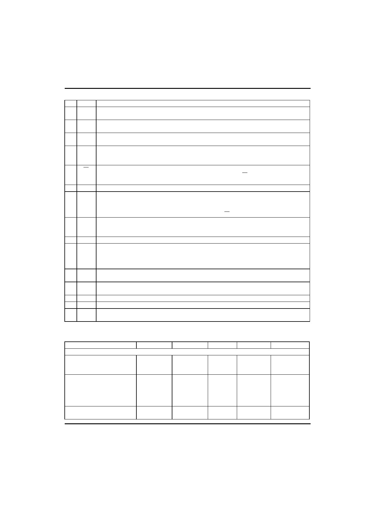
PIN NAME
DESCRIPTION
14 SKG High current ground pin for the speaker amplifier output stage. The SKG voltage should be within
10mV of the ground voltage at pin 22.
15 SKO Speaker amplifier output. The SKO pin will source and sink up to 100mA when ac coupled to the
speaker. The speaker amplifier gain is internally set at 34dB(50V/V).
16 V+ Input DC supply voltage. V+ can be powered from Tip and Ring if an ac decoupling inductor is used
to prevent loading ac line signals. The required V+ voltage is 6.0V to 11V(7.5V nominal ) at 7.0mA.
17 AGC A capacitor from this pin to VB stabilizes the speaker amplifier gain control loop, and additionally
controls the attack and decay time of this circuit. The gain control loop limits the speaker amplifier
input to prevent clipping at SKO. The internal resistance at AGC pin is nominally 110k ohms.
18 CS Digital chip select input. When at a logic "0" (<0.7V) the VCC regulator is enabled. When at a logic
"1" (>1.6V),the chip is in the standby mode drawing 0.5mA.An open CS pin is a logic "0".Input
impedance is nominally 140k ohms. The input voltage should not exceed 11V.
19 SKI Input to the speaker amplifier. Input impedance is nominally 20k ohms.
20 VCC A 5.4V regulated output which powers all circuits except the speaker amplifier output stage. VCC can
be used to power external circuitry such as a microprocessor(3.0mA max.) A filter capacitor is
required. The UTC MC34018 can be powered by a separate regulated supply by connecting V+ and
VCC to a voltage between 4.5V and 6.5V while maintaining CS at a logic "1".
21 VB An output voltage equal to approximately VCC/2 which series as an analog ground for the
speakerphone system. Up to 1.5mA of external load current may be sourced from VB. Output
impedance is 250 ohms. A filter capacitor is required.
22 GND Ground pin for the IC(except the speaker amplifier)
23 XDC Transmit detector output. A resistor and capacitor at his pin hold the system in the transmit mode
during pauses between words or phrases. When the XDC pin voltage decays to ground, the
attenuators switch from the transmit mode to idle mode. The internal resistor at XDC is nominally
2.6k ohms(see fig.1).
24 VLC Volume control input>connecting this pin to the slider of a variable resistor provides receive mode
volume control. The VLC pin voltage should be less than or equal to VB.
25 ACF Attenuator control filter. A capacitor connected to this pin reduces noise transient as the attenuator
control switches level of attenuation.
26 RXO Output of the receive attenuator. Normally this pin is ac coupled to the input of the speaker amplifier.
27 RXI Input of the receive attenuator. Input impedance is nominally is 5.0k ohms.
28 RRX A resistor to ground determines the nominal gain of the receive attenuator. The receive channel gain
is directly proportional to the RRX resistance.
ELECTRICAL CHARACTERISTICS(referred to fig. 1)
PARAMETER
SYMBOL
MIN
SUPPLY VOLTAGES
V+ Supply Current
IV+
V+=11V,Pin 18=0.7V
V+=11V,Pin 18=1.6V
VCC Voltage(V+=7.5V)
Vcc
4.9
Line
∆VccLN
Regulation(6.5V<V+<11V)
RoVcc
Output Resistance(ICC=3mA)
Vccsat
Dropout Voltage(V+=5.0V)
VB Voltage(V+=7.5V)
Vb
2.5
Output Resistance(IB=1.7mA)
Rovb
TYP
5.4
65
6.0
80
2.9
250
UTC UNISONIC TECHNOLOGIES
MAX
UNIT
9.0
mA
800
µA
5.9
Vdc
150
mV
20
ohms
300
mV
3.3
Vdc
ohms
CO., LTD. 3
QW-R108-006,A
Share Link: 