74ABT16821A 查看數據表(PDF) - Philips Electronics
零件编号
产品描述 (功能)
比赛名单
74ABT16821A
Philips Electronics

74ABT16821A Datasheet PDF : 10 Pages
| |||
Philips Semiconductors
20-bit bus-interface D-type flip-flop;
positive-edge trigger (3-State)
Product specification
74ABT16821A
74ABTH16821A
FEATURES
• 20-bit positive-edge triggered register
• Multiple VCC and GND pins minimize switching noise
• Live insertion/extraction permitted
• Power-up reset
• Power-up 3-State
• 74ABTH16821A incorporates bus-hold data inputs which
eliminate the need for external pull-up resistors to hold unused
inputs
• Output capability: +64mA/-32mA
• Latch-up protection exceeds 500mA per JEDEC Std 17
• ESD protection exceeds 2000V per MIL STD 883 Method 3015
and 200V per Machine Model
DESCRIPTION
The 74ABT16821A high-performance BiCMOS device combines
low static and dynamic power dissipation with high speed and high
output drive.
The 74ABT16821A has two 10-bit, edge triggered registers, with
each register coupled to a 3-State output buffer. The two sections of
each register are controlled independently by the clock (nCP) and
Output Enable (nOE) control gates.
Each register is fully edge triggered. The state of each D input, one
set-up time before the Low-to-High clock transition, is transferred to
the corresponding flip-flop’s Q output.
The 3-State output buffers are designed to drive heavily loaded
3-State buses, MOS memories, or MOS microprocessors.
The active Low Output Enable (nOE) controls all ten 3-State buffers
independent of the register operation. When nOE is Low, the data in
the register appears at the outputs. When nOE is High, the outputs
are in high impedance “off” state, which means they will neither drive
nor load the bus.
Two options are available, 74ABT16821A which does not have the
bus-hold feature and 74ABTH16821A which incorporates the
bus-hold feature.
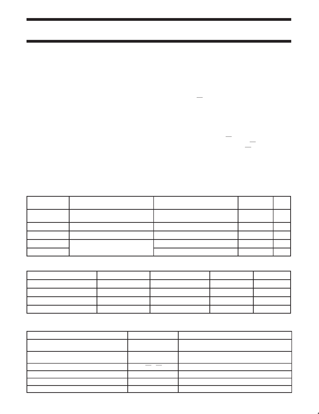
QUICK REFERENCE DATA
SYMBOL
PARAMETER
tPLH
tPHL
CIN
COUT
ICCZ
ICCL
Propagation delay
nCP to nQx
Input capacitance
Output capacitance
Quiescent supply current
CONDITIONS
Tamb = 25°C; GND = 0V
CL = 50pF; VCC = 5V
VI = 0V or VCC
VO = 0V or VCC; 3-State
Outputs disabled; VCC = 5.5V
Outputs LOW; VCC = 5.5V
TYPICAL
2.4
2.0
3
7
500
10
UNIT
ns
pF
pF
µA
mA
ORDERING INFORMATION
PACKAGES
56-Pin Plastic SSOP Type III
56-Pin Plastic TSSOP Type II
56-Pin Plastic SSOP Type III
56-Pin Plastic TSSOP Type II
TEMPERATURE RANGE OUTSIDE NORTH AMERICA
–40°C to +85°C
74ABT16821A DL
–40°C to +85°C
74ABT16821A DGG
–40°C to +85°C
74ABTH16821A DL
–40°C to +85°C
74ABTH16821A DGG
NORTH AMERICA
BT16821A DL
BT16821A DGG
BH16821A DL
BH16821A DGG
DWG NUMBER
SOT371-1
SOT364-1
SOT371-1
SOT364-1
PIN DESCRIPTION
PIN NUMBER
55, 54, 52, 51, 49, 48, 47, 45, 44, 43,
42, 41, 40, 38, 37, 36, 34, 33, 31, 30
2, 3, 5, 6, 8, 9, 10, 12, 13, 14,
15, 16, 17, 19, 20, 21, 23, 24, 26, 27
1, 28
56, 29
4, 11, 18, 25, 32, 39, 46, 53
7, 22, 35, 50
1998 Feb 27
SYMBOL
1D0 - 1D9
2D0 - 2D9
1Q0 - 1Q9
2Q0 - 2Q9
1OE, 2OE
1CP, 2CP
GND
VCC
2
Data inputs
FUNCTION
Data outputs
Output enable inputs (active-Low)
Clock pulse inputs (active rising edge)
Ground (0V)
Positive supply voltage
853-1796 19026
Share Link: