74ABT16821A 查看數據表(PDF) - Philips Electronics
零件编号
产品描述 (功能)
比赛名单
74ABT16821A
Philips Electronics

74ABT16821A Datasheet PDF : 10 Pages
| |||
Philips Semiconductors
20-bit bus-interface D-type flip-flop;
positive-edge trigger (3-State)
Product specification
74ABT16821A
74ABTH16821A
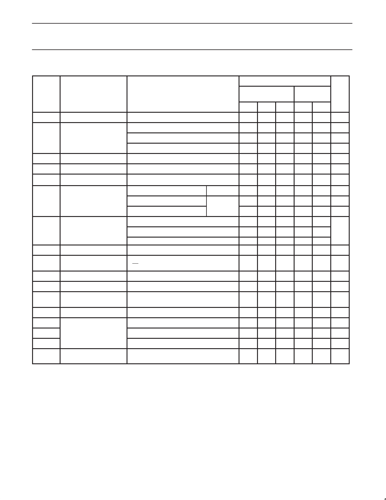
DC ELECTRICAL CHARACTERISTICS
LIMITS
SYMBOL
PARAMETER
TEST CONDITIONS
Tamb = +25°C
Tamb = -40°C
to +85°C
UNIT
Min Typ Max Min Max
VIK
VOH
VOL
VRST
II
Input clamp voltage
High-level output voltage
Low-level output voltage
Power-up output voltage3
Input leakage current
VCC = 4.5V; IIK = -18mA
VCC = 4.5V; IOH = -3mA; VI = VIL or VIH
VCC = 5.0V; IOH = -3mA; VI = VIL or VIH
VCC = 4.5V; IOH = -32mA; VI = VIL or VIH
VCC = 4.5V; IOL = 64mA; VI = VIL or VIH
VCC = 5.5V; IO = 1mA; VI = GND or VCC
VCC = 5.5V; VI = VCC or GND
–0.9 –1.2
–1.2 V
2.5 2.9
2.5
V
3.0 3.4
3.0
V
2.0 2.4
2.0
V
0.36 0.55
0.55 V
0.13 0.55
0.55 V
±0.01 ±1.0
±1.0 µA
II
Input leakage current
74ABTH16821A
VCC = 5.5V; VI = VCC or GND
VCC = 5.5V; VI = VCC
VCC = 5.5V; VI = 0
Control pins
Data pins
±0.01 ±1
0.01 1
–1 –3
±1 µA
1
µA
–5 µA
IHOLD
IOFF
Bus Hold current inputs5
74ABTH16821A
Power-off leakage current
VCC = 4.5V; VI = 0.8V
VCC = 4.5V; VI = 2.0V
VCC = 5.5V; VI = 0 to 5.5V
VCC = 0.0V; VO or VI ≤ 4.5V
35
35
–75
–75
µA
±800
±5.0 ±100
±100 µA
IPU/PD
Power-up/down 3-State
output current4
VCC = 2.1V; VO = 0.5V; VI = GND or VCC;
VOE = Don’t care
±5.0 ±50
±50 µA
IOZH 3-State output High current VCC = 5.5V; VO = 2.7V; VI = VIL or VIH
1.0 10
10 µA
IOZL 3-State output Low current VCC = 5.5V; VO = 0.5V; VI = VIL or VIH
–1.0 –10
–10 µA
ICEX
Output High leakage
current
VCC = 5.5V; VO = 5.5V; VI = GND or VCC
5.0 50
50 µA
IO
Output current1
VCC = 5.5V; VO = 2.5V
–50 –90 –180 –50 –180 mA
ICCH
VCC = 5.5V; Outputs High, VI = GND or VCC
0.5
1
1
mA
ICCL Quiescent supply current VCC = 5.5V; Outputs Low, VI = GND or VCC
10 19
19 mA
ICCZ
VCC = 5.5V; Outputs 3-State; VI = GND or VCC
0.5
1
1
mA
∆ICC
Additional supply current
per input pin2
VCC = 5.5V; one input at 3.4V, other inputs at
VCC or GND
0.25 1.5
1.5 mA
NOTES:
1. Not more than one output should be tested at a time, and the duration of the test should not exceed one second.
2. This is the increase in supply current for each input at 3.4V.
3. For valid test results, data must not be loaded into the flip-flops (or latches) after applying the power.
4. This parameter is valid for any VCC between 0V and 2.1V with a transition time of up to 10msec. From VCC = 2.1V to VCC = 5V a transition
time of up to 100µsec is permitted.
5. This is the bus hold overdrive current required to force the input to the opposite logic state.
1998 Feb 27
5
Share Link: