BS616LV1010 查看數據表(PDF) - Brilliance Semiconductor
零件编号
产品描述 (功能)
比赛名单
BS616LV1010 Datasheet PDF : 11 Pages
| |||
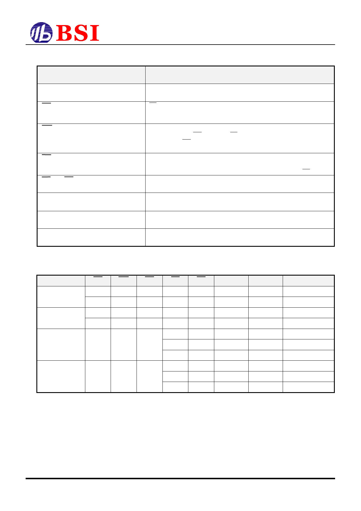
n PIN DESCRIPTIONS
BS616LV1010
Name
A0-A15 Address Input
Function
These 16 address inputs select one of the 65,536 x 16-bit in the RAM
CE Chip Enable Input
WE Write Enable Input
OE Output Enable Input
LB and UB Data Byte Control Input
CE is active LOW. Chip enable must be active when data read form or write to the
device. If chip enable is not active, the device is deselected and is in standby power
mode. The DQ pins will be in the high impedance state when the device is deselected.
The write enable input is active LOW and controls read and write operations. With the
chip selected, when WE is HIGH and OE is LOW, output data will be present on the
DQ pins; when WE is LOW, the data present on the DQ pins will be written into the
selected memory location.
The output enable input is active LOW. If the output enable is active while the chip is
selected and the write enable is inactive, data will be present on the DQ pins and they
will be enabled. The DQ pins will be in the high impendence state when OE is inactive.
Lower byte and upper byte data input/output control pins.
DQ0-DQ15 Data Input/Output
Ports
VCC
VSS
There 16 bi-directional ports are used to read data from or write data into the RAM.
Power Supply
Ground
n TRUTH TABLE
MODE
CE
WE
OE
LB
UB
Chip De-selected
H
X
X
X
X
(Power Down)
X
X
X
H
H
L
H
H
L
X
Output Disabled
L
H
H
X
L
L
L
Read
L
H
L
H
L
L
H
L
L
Write
L
L
X
H
L
L
H
NOTES: H means VIH; L means VIL; X means don’t care (Must be VIH or VIL state)
IO0~IO7
High Z
High Z
High Z
High Z
DOUT
High Z
DOUT
DIN
X
DIN
IO8~IO15
High Z
High Z
High Z
High Z
DOUT
DOUT
High Z
DIN
DIN
X
VCC CURRENT
ICCSB, ICCSB1
ICCSB, ICCSB1
ICC
ICC
ICC
ICC
ICC
ICC
ICC
ICC
R0201-BS616LV1010
2
Revision 2.6
May.
2006
Share Link: 