BS616LV1010 查看數據表(PDF) - Brilliance Semiconductor
零件编号
产品描述 (功能)
比赛名单
BS616LV1010 Datasheet PDF : 11 Pages
| |||
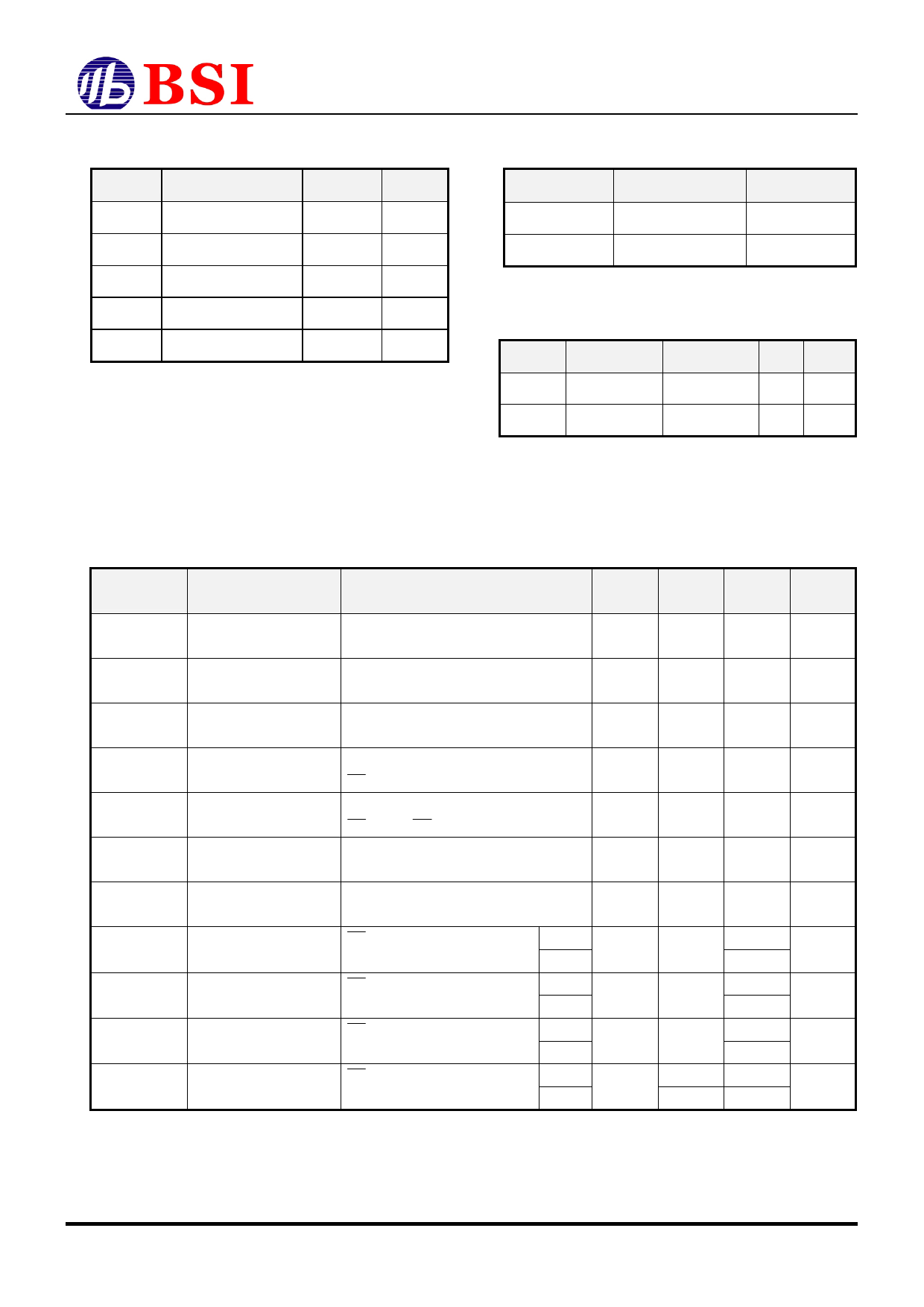
n ABSOLUTE MAXIMUM RATINGS (1)
SYMBOL PARAMETER
VTERM
TBIAS
Terminal Voltage with
Respect to GND
Temperature Under
Bias
TSTG
Storage Temperature
PT
Power Dissipation
IOUT
DC Output Current
RATING UNITS
-0.5(2) to 7.0
V
-40 to +125
OC
-60 to +150
OC
1.0
W
20
mA
1. Stresses greater than those listed under ABSOLUTE
MAXIMUM RATINGS may cause permanent damage to the
device. This is a stress rating only and functional operation of
the device at these or any other conditions above those
indicated in the operational sections of this specification is not
implied. Exposure to absolute maximum rating conditions for
extended periods may affect reliability.
2. –2.0V in case of AC pulse width less than 30 ns.
BS616LV1010
n OPERATING RANGE
RANG
Commercial
Industrial
AMBIENT
TEMPERATURE
0OC to + 70OC
-40OC to + 85OC
VCC
2.4V ~ 5.5V
2.4V ~ 5.5V
n CAPACITANCE (1) (TA = 25OC, f = 1.0MHz)
SYMBOL PAMAMETER CONDITIONS MAX. UNITS
CIN
Input
Capacitance
CIO
Input/Output
Capacitance
VIN = 0V
VI/O = 0V
6
pF
8
pF
1. This parameter is guaranteed and not 100% tested.
n DC ELECTRICAL CHARACTERISTICS (TA = -40OC to +85OC)
PARAMETER
NAME
PARAMETER
VCC
Power Supply
TEST CONDITIONS
MIN. TYP.(1) MAX. UNITS
2.4
--
5.5
V
VIL
Input Low Voltage
-0.5(2)
--
0.8
V
VIH
Input High Voltage
IIL
Input Leakage Current
VIN = 0V to VCC
CE= VIH
ILO
VI/O = 0V to VCC,
Output Leakage Current
CE= VIH or OE = VIH
VOL
Output Low Voltage
VCC = Max, IOL = 2.0mA
2.2
--
VCC+0.3(3)
V
--
--
1
uA
--
--
1
uA
--
--
0.4
V
VOH
Output High Voltage
VCC = Min, IOH = -1.0mA
ICC(5)
ICC1
ICCSB
ICCSB1(6)
Operating Power Supply
Current
CE = VIL,
IIO = 0mA, f = FMAX(4)
Operating Power Supply CE = VIL,
Current
IIO = 0mA, f = 1MHz
Standby Current – TTL
CE = VIH,
IIO = 0mA
Standby Current – CMOS CE≧VCC-0.2V
VIN≧VCC-0.2V or VIN≦0.2V
1. Typical characteristics are at TA=25OC and not 100% tested.
2. Undershoot: -1.0V in case of pulse width less than 20 ns.
3. Overshoot: VCC+1.0V in case of pulse width less than 20 ns.
4. FMAX=1/tRC(MIN.).
5. ICC (MAX.) is 24mA/44mA at VCC=3.0V/5.0V and TA=70OC.
6. ICCSB1(MAX.) is 0.5uA/3.0uA at VCC=3.0V/5.0V and TA=70OC.
R0201-BS616LV1010
3
2.4
VCC=3.0V
--
VCC=5.0V
VCC=3.0V
--
VCC=5.0V
VCC=3.0V
--
VCC=5.0V
VCC=3.0V
--
VCC=5.0V
--
--
--
--
0.02
0.4
--
V
25
mA
45
2
mA
5
0.5
mA
1.0
1.5
uA
5.0
Revision 2.6
May.
2006
Share Link: 