IDT74FCT3244APGG 查看數據表(PDF) - Integrated Device Technology
零件编号
产品描述 (功能)
比赛名单
IDT74FCT3244APGG Datasheet PDF : 6 Pages
| |||
IDT74FCT3244/A
3.3V CMOS OCTAL BUFFER/LINE DRIVER
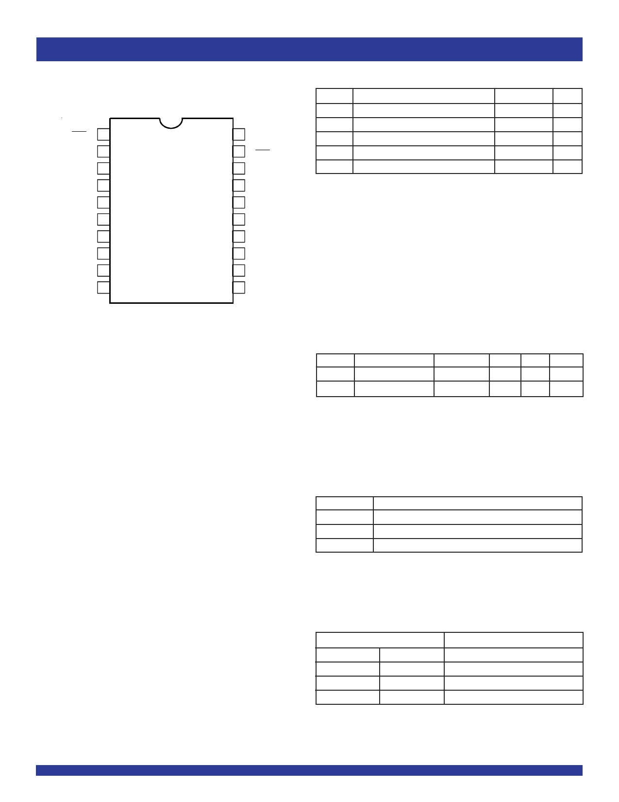
PIN CONFIGURATION
1OE
1
1A1
2
2Y 4
3
1 A2
4
2Y 3
5
1A3
6
2Y 2
7
1A4
8
2Y1
9
GND
10
20 Vcc
19 2OE
18 1Y1
17 2A4
16 1Y2
15 2A 3
14 1Y 3
13 2A 2
12 1Y4
11 2A1
SOIC/ SSOP/ QSOP/ TSSOP
TOP VIEW
INDUSTRIAL TEMPERATURE RANGE
ABSOLUTE MAXIMUM RATINGS(1)
Symbol Description
Max
Unit
VTERM(2) Terminal Voltage with Respect to GND –0.5 to +4.6 V
VTERM(3) Terminal Voltage with Respect to GND
–0.5 to +7
V
VTERM(4) Terminal Voltage with Respect to GND –0.5 to VCC+0.5 V
TSTG StorageTemperature
–65 to +150 °C
IOUT DC Output Current
–60 to +60 mA
NOTES:
1. Stresses greater than those listed under ABSOLUTE MAXIMUM RATINGS may
cause permanent damage to the device. This is a stress rating only and functional
operation of the device at these or any other conditions above those indicated in
the operational sections of this specification is not implied. Exposure to absolute
maximum rating conditions for extended periods may affect reliability.
2. VCC terminals.
3. Input terminals.
4. Outputs and I/O terminals.
CAPACITANCE (TA = +25°C, F = 1.0MHz)
Symbol
Parameter(1)
Conditions Typ. Max. Unit
CIN
Input Capacitance
VIN = 0V
3.5
6
pF
COUT
Output Capacitance VOUT = 0V
4
8
pF
NOTE:
1. This parameter is measured at characterization but not tested.
PIN DESCRIPTION
Pin Names
xOE
Description
3–State Output Enable Inputs (Active LOW)
xAx
Data Inputs
xYx
3-State Outputs
FUNCTION TABLE(1)
Inputs
xOE
xAx
L
L
L
H
H
X
NOTE:
1. H = HIGH Voltage Level
X = Don’t Care
L = LOW Voltage Level
Z = High Impedance
2
Outputs
xYx
L
H
Z
Share Link: 