IDT74FCT3244APGG 查看數據表(PDF) - Integrated Device Technology
零件编号
产品描述 (功能)
比赛名单
IDT74FCT3244APGG Datasheet PDF : 6 Pages
| |||
IDT74FCT3244/A
3.3V CMOS OCTAL BUFFER/LINE DRIVER
INDUSTRIAL TEMPERATURE RANGE
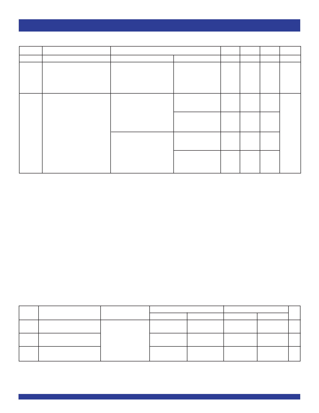
POWER SUPPLY CHARACTERISTICS
Symbol
Parameter
Test Conditions(1)
ICC
Quiescent Power Supply Current
VCC = Max.
ICCD
Dynamic Power Supply
Current(4)
VCC = Max.
Outputs Open
xOE = GND
One Input Toggling
50% Duty Cycle
IC
Total Power Supply Current(6)
VCC = Max.
Outputs Open
fI = 10MHz
50% Duty Cycle
xOE = GND
One Bit Toggling
VCC = Max.
Outputs Open
fI = 2.5MHz
50% Duty Cycle
xOE = GND
Eight Bits Toggling
VIN = VCC - 0.6V
VIN = VCC
VIN = GND
VIN = VCC
VIN = GND
VIN = VCC - 0.6V
VIN = GND
VIN = VCC
VIN = GND
VIN = VCC - 0.6V
VIN = GND
Min. Typ.(2) Max.
Unit
—
2
30
µA
—
60
85
µA/
MHz
—
0.6
0.9
mA
—
0.6
0.9
—
1.2
1.7(5)
—
1.2
1.8(5)
NOTES:
1. For conditions shown as Min. or Max., use appropriate value specified under Electrical Characteristics for the applicable device type.
2. Typical values are at VCC = 3.3V, +25°C ambient.
3. Per TTL driven input. All other inputs at VCC or GND.
4. This parameter is not directly testable, but is derived for use in Total Power Supply Calculations.
5. Values for these conditions are examples of ∆ICC formula. These limits are guaranteed but not tested.
6. IC = IQUIESCENT + IINPUTS + IDYNAMIC
IC = ICC + ∆ICC DHNT + ICCD (fCPNCP/2 + fiNi)
ICC = Quiescent Current (ICC, ICCH, and ICCZ)
∆ICC = Power Supply Current for a TTL High Input
DH = Duty Cycle for TTL Inputs High
NT = Number of TTL Inputs at DH
ICCD = Dynamic Current caused by an Input Transition Pair (HLH or LHL)
fCP = Clock Frequency for register devices (zero for non-register devices)
NCP = Number of clock inputs at fCP
fi = Input Frequency
Ni = Number of Inputs at fi
SWITCHING CHARACTERISTICS OVER OPERATING RANGE(1)
Symbol
tPLH
tPHL
tPZH
tPZL
tPHZ
tPLZ
Parameter
Propagation Delay
xAx to xYx
Output Enable Time
Output Disable Time
Condition(2)
CL = 50pF
RL = 500Ω
74FCT3244
Min.(3)
Max.
1.5
6.5
1.5
8
1.5
7
74FCT3244A
Min.(3)
Max.
Unit
1.5
4.8
ns
1.5
6.2
ns
1.5
5.6
ns
NOTES:
1. Propagation Delays and Enable/Disable times are with VCC = 3.3V ±0.3V, Normal Range. For VCC = 2.7V to 3.6V, Extended Range, all Propagation Delays and Enable/
Disable times should be degraded by 20%.
2. See test circuit and waveforms.
3. Minimum limits are guaranteed but not tested on Propagation Delays.
4
Share Link: 