MX10FMAXDPC 查看數據表(PDF) - Macronix International
零件编号
产品描述 (功能)
比赛名单
MX10FMAXDPC Datasheet PDF : 24 Pages
| |||
MX10FMAXDPC
MX10FMAXDQC
5. PROGRAMMING SPECIFICATION
MX10FMAX has two programming modes, which depends on the P2.6 pin. If P2.6 = 1, then it is in parallel program-
ming mode, if not, then it is in serial programming mode.
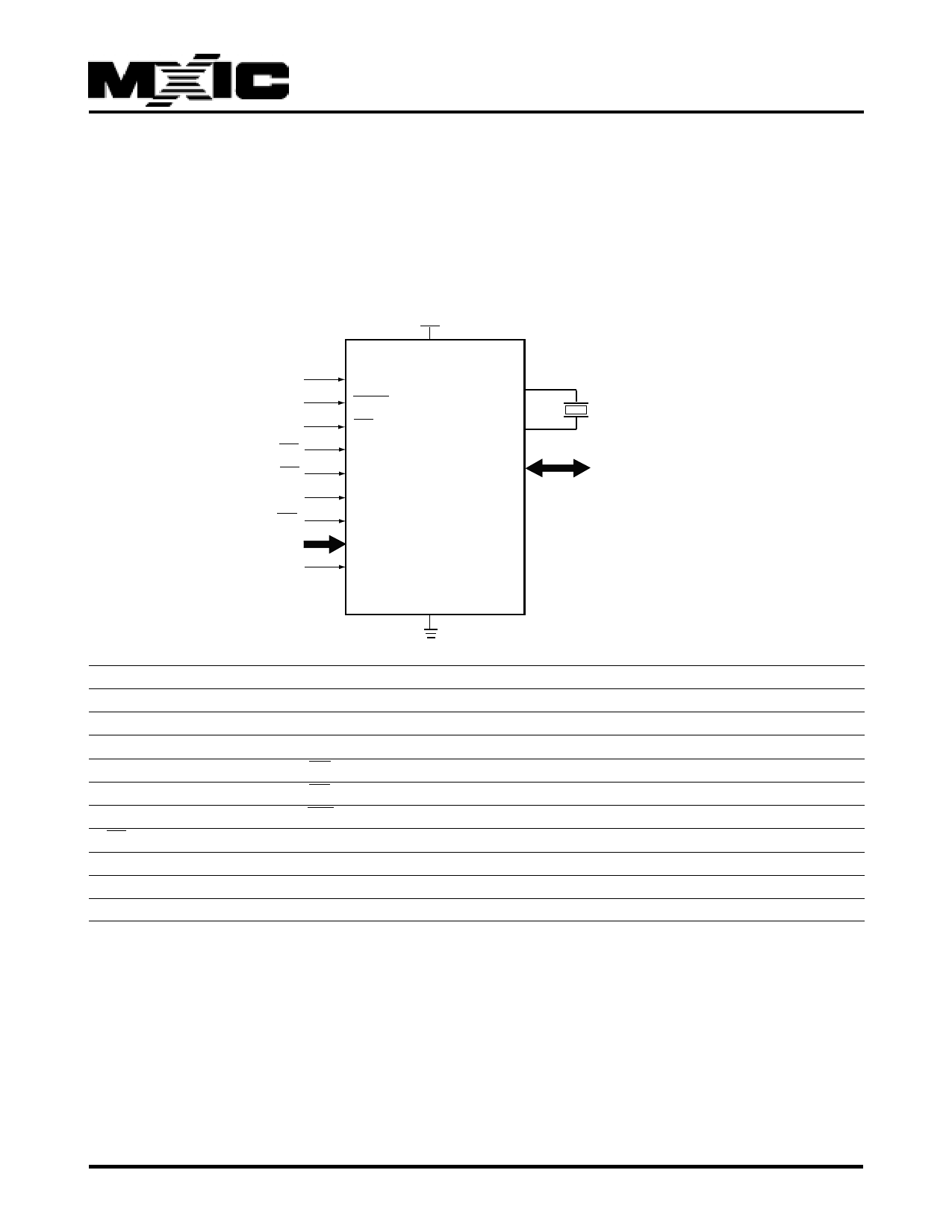
5.1 Parallel Programming Mode
1
0
12.5~13V,5/6.25/4.5V
CE
OE
1
WE
A[15:0]
MS[2:0]
4.5/5/6.25V
VDD
RST
PSEN
XTAL1
EA
XTAL2
P3.3
P2.7
P0[7:0]
P2.6
ALE
P3[5:4],P2[5:0],P[7:0]
P3.7,P3.1, P3.0
VSS
4~6MHz
Q[7:0]
PIN NAME
P1.0 ~ P1.7
P2.0 ~ P2.5, P3.4 ~ P3.5
P0.0 ~ P0.7
P3.3
P2.7
ALE
EA
P3.7, P3.1, P3.0
VDD
GND
SYMBOL
A0 ~A7
A8 ~ A13, A14 ~A15
Q0 ~ Q7
CE
OE
WE
Vpp
MS2 ~ MS0
VDD
GND
Notice for speed progamming
FUNCTION
Input low order address bits
Input high order address bits
Data Input/Output
Chip Enable Input
Output Enable Input
Write Enable Input
Program Supply Voltage, 12.5 ~13Volts
Flash Mode Selection
Power Supply Voltage (+5V)
Ground Pin
P/N:PM1053 Specifications subject to change without notice, contact your sales representatives for the most update information. REV. 1.0, DEC. 10, 2003
6
Share Link: 