RMLV0408E 查看數據表(PDF) - Renesas Electronics
零件编号
产品描述 (功能)
比赛名单
RMLV0408E Datasheet PDF : 12 Pages
| |||
RMLV0408E Series
AC Characteristics
Test Conditions (Vcc = 2.7V ~ 3.6V, Ta = -40 ~ +85°C)
Input pulse levels: VIL = 0.4V, VIH = 2.4V
Input rise and fall time: 5ns
Input and output timing reference level: 1.4V
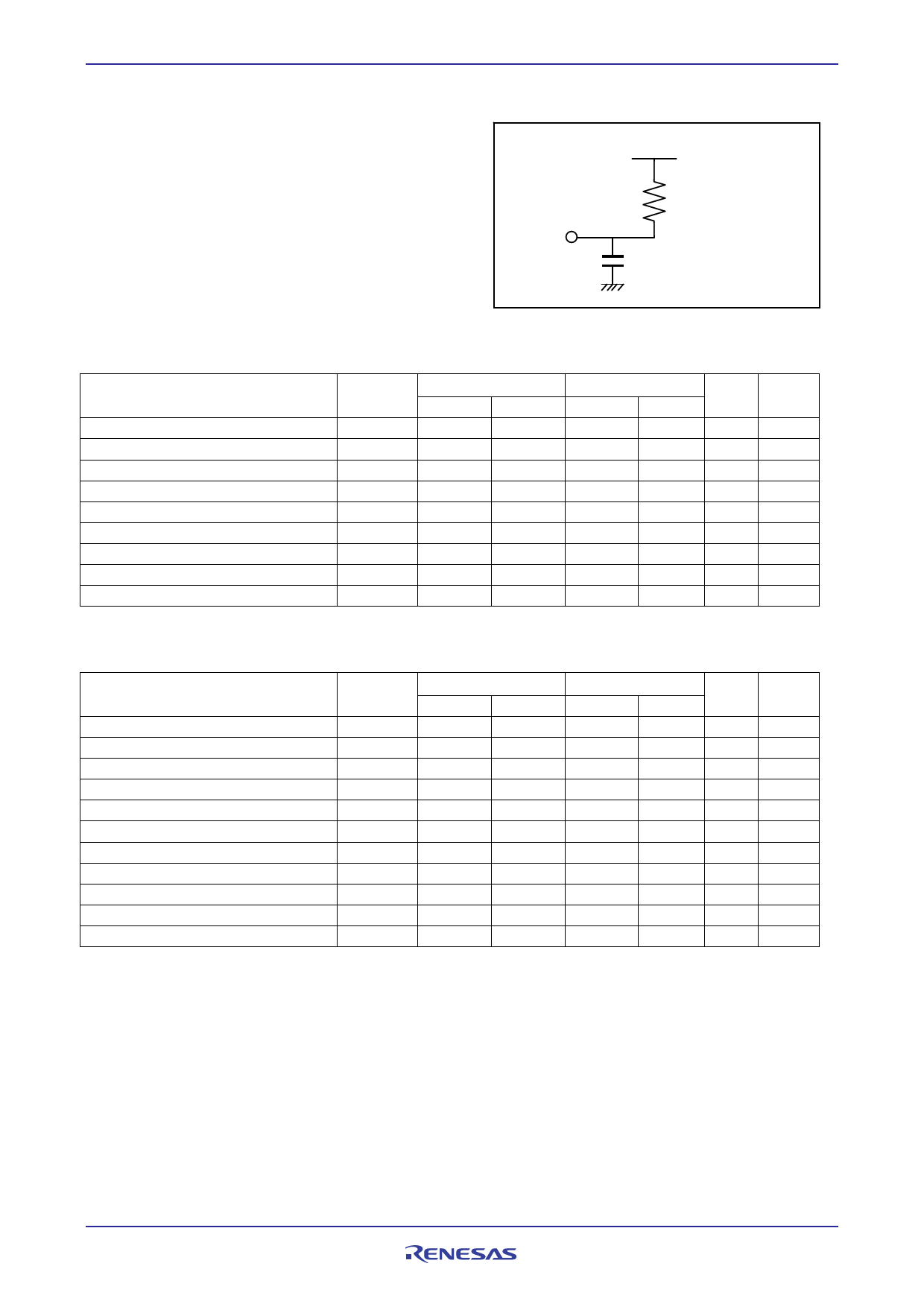
Output load: See figures (Including scope and jig)
I/O
Preliminary
1.4V
RL = 500 ohm
CL = 30 pF (-4S2)
CL = 50 pF (-5S2)
Read Cycle
Parameter
Read cycle time
Address access time
Chip select access time
Output enable to output valid
Output hold from address change
Chip select to output in low-Z
Output enable to output in low-Z
Chip deselect to output in high-Z
Output disable to output in high-Z
Symbol
tRC
tAA
tACS
tOE
tOH
tCLZ
tOLZ
tCHZ
tOHZ
RMLV0408EG**-4S2
Min.
Max.
45
─
─
45
─
45
─
22
10
─
10
─
5
─
0
18
0
18
RMLV0408EG**-5S2 Unit
Min.
Max.
55
─
ns
─
55
ns
─
55
ns
─
30
ns
10
─
ns
10
─
ns
5
─
ns
0
20
ns
0
20
ns
Note
7,8
7,8
7,8,9
7,8,9
Write Cycle
Parameter
Symbol
RMLV0408EG**-4S2
RMLV0408EG**-5S2
Unit
Min.
Max.
Min.
Max.
Note
Write cycle time
tWC
45
─
55
─
ns
Address valid to write end
tAW
35
─
50
─
ns
Chip select to write end
tCW
35
─
50
─
ns
Write pulse width
tWP
35
─
40
─
ns
10
Address setup time to write start
tAS
0
─
0
─
ns
Write recovery time from write end
tWR
0
─
0
─
ns
Data to write time overlap
tDW
25
─
25
─
ns
Data hold from write end
tDH
0
─
0
─
ns
Output enable from write end
tOW
5
─
5
─
ns
7
Output disable to output in high-Z
tOHZ
0
18
0
20
ns
7,9
Write to output in high-Z
tWHZ
0
18
0
20
ns
7,9
Note 7. This parameter is sampled and not 100% tested.
8. At any given temperature and voltage condition, tCHZ max is less than tCLZ min, and tOHZ max is less than tOLZ
min, for any device.
9. tCHZ, tOHZ and tWHZ are defined as the time when the I/O pins enter a high-impedance state and are not
referred to the I/O levels.
10. tWP is the interval between write start and write end.
A write starts when both of CS# and WE# become active
A write is performed during the overlap of a low CS#, a low WE#
A write ends when any of CS#, WE# becomes inactive.
R10DS0217EJ0001 Rev.0.01
2013.09.10
Page 5 of 10
Share Link: 