AD8153 查看數據表(PDF) - Analog Devices
零件编号
产品描述 (功能)
比赛名单
AD8153 Datasheet PDF : 24 Pages
| |||
AD8153
I2C DATA WRITE
To write data to the AD8153 register set, a microcontroller, or
any other I2C master, needs to send the appropriate control
signals to the AD8153 slave device. The steps that need to be
followed are listed below, where the signals are controlled by the
I2C master unless otherwise specified. A diagram of the procedure
is shown in Figure 32.
1. Send a start condition (while holding the SCL line high, pull
the SDA line low).
2. Send the AD8153 part address (seven bits) whose upper
four bits are the static value b1001 and whose lower three
bits are controlled by the input pins I2C_A[2:0]. This
transfer should be MSB first.
3. Send the write indicator bit (0).
4. Wait for the AD8153 to acknowledge the request.
5. Send the register address (eight bits) to which data is to be
written. This transfer should be MSB first.
6. Wait for the AD8153 to acknowledge the request.
7. Send the data (eight bits) to be written to the register whose
address was set in Step 5. This transfer should be MSB first.
8. Wait for the AD8153 to acknowledge the request.
9. Send a stop condition (while holding the SCL line high, pull
the SDA line high) and release control of the bus.
SCL
Data Sheet
10. Send a repeated start condition (while holding the SCL line
high, pull the SDA line low) and continue with Step 2 in this
procedure to perform another write.
11. Send a repeated start condition (while holding the SCL line
high, pull the SDA line low) and continue with Step 2 of the
read procedure (in the I2C Data Read section) to perform a
read from another address.
12. Send a repeated start condition (while holding the SCL line
high, pull the SDA line low) and continue with step 8 of the
read procedure (in the I2C Data Read section) to perform a
read from the same address set in Step 5.
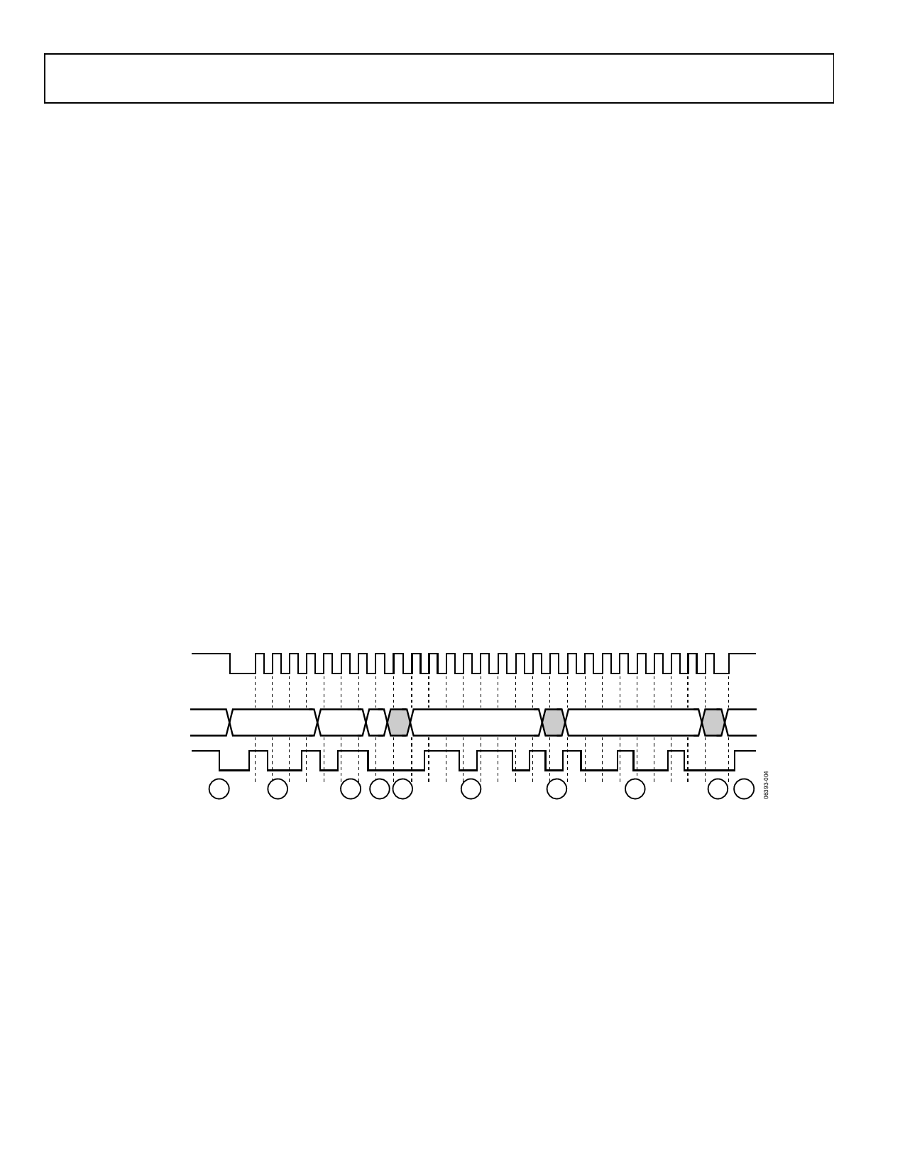
The AD8153 write process is shown in Figure 32. The SCL
signal is shown along with a general write operation and a
specific example. In the example, data 0x92 is written to
Address 0x6D of an AD8153 part with a part address of 0x4B.
The part address is seven bits wide and is composed of the
AD8153 static upper four bits (b1001) and the pin
programmable lower three bits (I2C_ADDR[2:0]). In this
example, the I2C_ADDR bits are set to b011. In Figure 32, the
corresponding step number is visible in the circle under the
waveform. The SCL line is driven by the I2C master and never
by the AD8153 slave. As for the SDA line, the data in the shaded
polygons is driven by the AD8153, whereas the data in the non-
shaded polygons is driven by the I2C master. The end phase case
shown is that of 9a.
It is important to note that the SDA line only changes when the
SCL line is low, except for the case of sending a start, stop, or
repeated start condition, Step 1 and Step 9 in this case.
SDA
(GENERAL CASE)
START
FIXED PART ADDR
ADDR
[2:0]
RW ACK
REGISTER ADDR
SDA
(EXAMPLE)
1
2
2
34
5
Figure 32. I2C Write Diagram
ACK
6
DATA
7
ACK STOP
8 9a
Rev. A | Page 16 of 24
Share Link: 