AD8153 查看數據表(PDF) - Analog Devices
零件编号
产品描述 (功能)
比赛名单
AD8153 Datasheet PDF : 24 Pages
| |||
AD8153
Data Sheet
INTERFACING TO THE AD8153
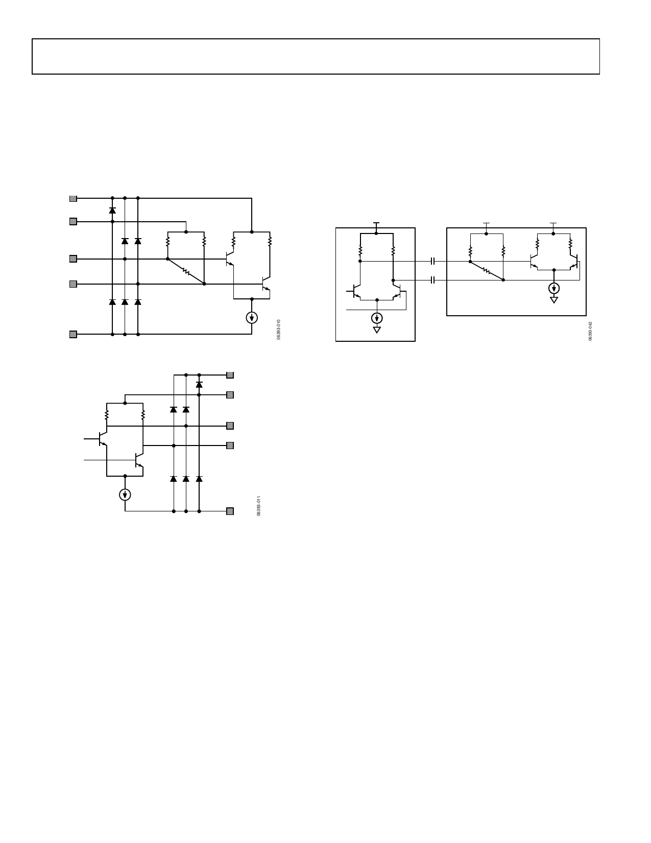
TERMINATION STRUCTURES
To determine the best strategy for connecting to the high speed
pins of the AD8153, the user must first be familiar with the on-
chip termination structures. The AD8153 contains two types of
these structures: one type for input ports and one type for output
ports (see Figure 37 and Figure 38).
VCC
VTTI
55Ω
55Ω
IPX
1173Ω
INX
AC Coupling
One way to simplify the input circuit and make it compatible
with a wide variety of driving devices is to use ac coupling. This
has the effect of isolating the dc common-mode levels of the
driver and the AD8153 input circuitry. AC coupling requires a
capacitor in series with each single-ended input signal, as shown
in Figure 39. This should be done in a manner that does not
interfere with the high speed signal integrity of the PCB.
VCC
VTTI
VCC
50Ω
50Ω
CP
IP
55Ω
55Ω
CN
IN 1173Ω
AD8153
VEE
VEE
DRIVER
Figure 37. Receiver Simplified Diagram
Figure 39. AC-Coupling Input Signal of AD8153
50Ω
50Ω
VIP
VIN
VCC
VTTO
OPX
ONX
IT
VEE
Figure 38. Transmitter Simplified Diagram
When ac coupling is used, the common-mode level at the input
of the device is equal to VTTI. The single-ended input signal
swings above and below VTTI equally. The user can then use
the specifications in Table 1 to determine the input signal swing
levels that satisfy the input range of the AD8153.
If dc coupling is required, determining the input common-
mode level is less straightforward because the configuration of
the driver must also be considered. In most cases, the user
would set VTTI on the AD8153 to the same level as the driver
output termination voltage. This prevents a continuous dc
current from flowing between the two supply nets. As a
practical matter, both devices can be terminated to the same
physical supply net.
For input ports, the termination structure consists of two 55 Ω
Consider the following example: a driver is dc-coupled to the
resistors connected to a termination supply and an 1173 Ω
input of the AD8153. The AD8153 input termination voltage
resistor connected across the differential inputs, the latter being
(VTTI) and the driver output termination voltage (VTTOD) are both
a result of the finite differential input impedance of the equalizer.
set to the same level; that is, VTTI = VTTOD = 3.3 V. If an 800 mV
For output ports, there are two 50 Ω resistors connected to the
termination supply. Note that the differential input resistance
for both structures is the same, 100 Ω.
INPUT COMPLIANCE
differential p-p swing is desired, the total output current of the
driver is 16 mA. At balance, the output current is divided evenly
between the two sides of the differential signal path, 8 mA to each
side. This 8 mA of current flows through the parallel combina-
tion of the 55 Ω input termination resistor on the AD8153 and
The range of allowable input voltages is determined by the
the 50 Ω output termination resistor on the driver, resulting in a
fundamental limitations of the active input circuitry. This range
common-mode level of
of signals is normally a function of the common-mode level of
the input signal, the signal swing, and the supply voltage. For a
given input signal swing, there is a range of common-mode
voltages that keeps the high and low voltage excursions within
acceptable limits. Similarly, for a given common-mode input
VTTI − 8 mA × (50 Ω || 55 Ω) = VTTI − 209 mV
The user can then determine the allowable range of values for VTTI
that meets the input compliance range based on an 800 mV p-p
differential swing.
voltage, there is a maximum acceptable input signal swing.
There is also a minimum signal swing that the active input
circuitry can resolve reliably. The specifications are found in
Table 1.
Rev. A | Page 20 of 24
Share Link: 