AD8158 查看數據表(PDF) - Analog Devices
零件编号
产品描述 (功能)
比赛名单
AD8158 Datasheet PDF : 36 Pages
| |||
AD8158
Parameter
Supply Current
ICC
ITTO
ITTI
IDVCC
Supply Current
ICC
ITTO
ITTI
IDVCC
THERMAL CHARACTERISTICS
Operating Temperature Range
θJA
θJC
Maximum Junction Temperature
LOGIC INPUT CHARACTERISTICS3
Input High (VIH)
Input Low (VIL)
Input High (VIH)
Input Low (VIL)
Conditions
DC-coupled inputs/outputs, 400 mV I/O swings (800 mV
p-p differential), 50 Ω far-end terminations
LB_x = 1, PE = 6 dB on all ports, dc-coupled
inputs/outputs, 400 mV I/O swings (800 mV p-p
differential), 50 Ω far-end terminations
Still air; JEDEC four-layer test board, ePAD soldered
Still air; thermal resistance through exposed pad
I2C, SDA, SCL, control pins
DVCC = 3.3 V
DVCC = 3.3 V
DVCC = 1.8 V
DVCC = 1.8 V
Min
Typ
Max
Unit
354
450
mA
128
150
mA
94
107
mA
2
4
mA
730
850
mA
367
420
mA
95
107
mA
2
4
mA
−40
+85
°C
22.2
°C/W
1.4
°C/W
125
°C
0.7 × DVCC
DVCC
V
VEE
0.3 × DVCC V
0.8 × DVCC DVCC
V
VEE
0.2 × DVCC
V
1 Bicast is off, loopback is off on all ports, pre-emphasis is set to minimum on all ports, and equalization is set to minimum on all ports.
2 VICM is the input common-mode voltage.
3 EQ control pins (EQ_A0, EQ_A1, EQ_B0, EQ_B1, EQ_C0, EQ_C1) require 5 kΩ in series when DVCC > VCC.
I2C TIMING SPECIFICATIONS
SDA
tF
SCL
S
tLOW
tR
tSU;DAT
tF
tHD;STA
tHD;STA
tHD;DAT
tHIGH
tSU;STA
Sr
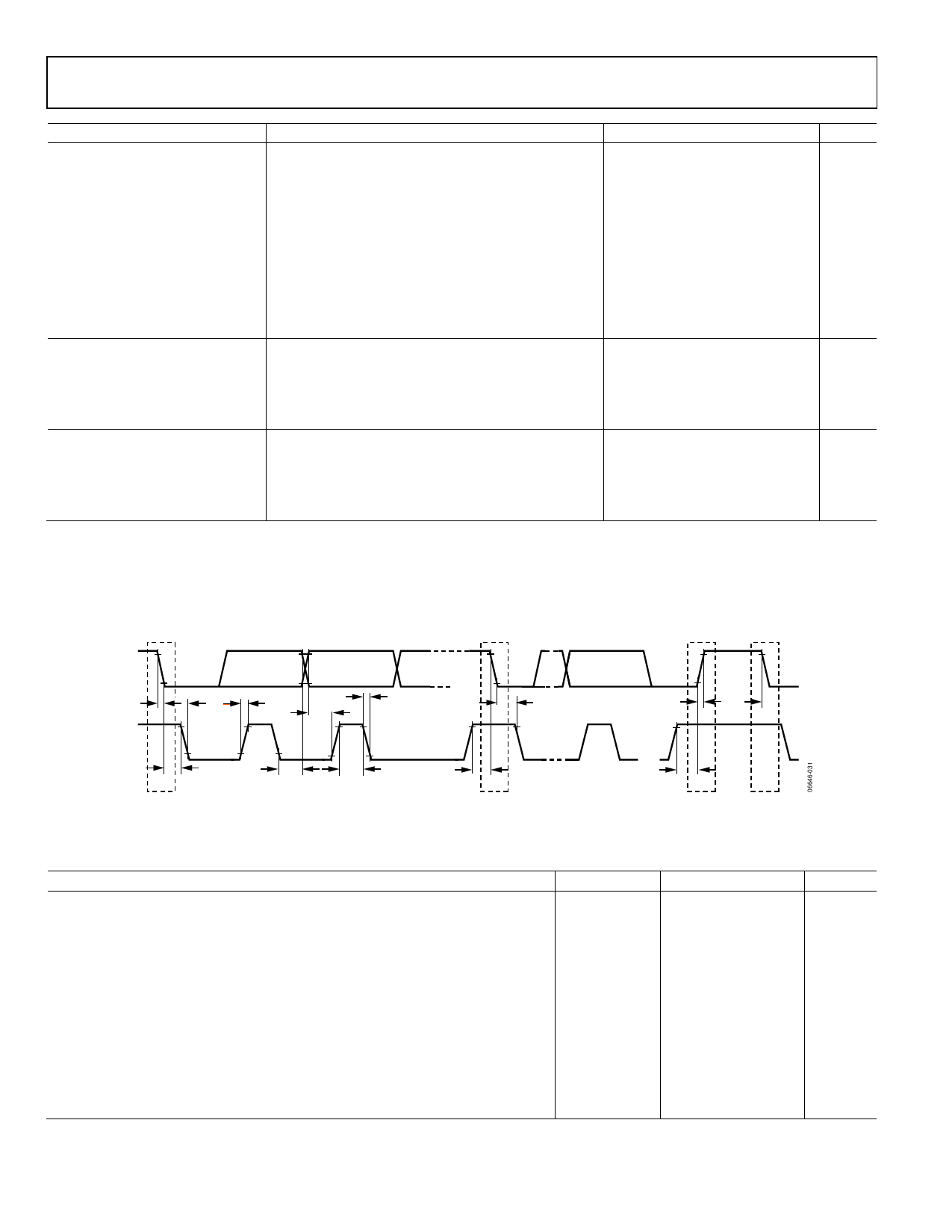
Figure 2. I2C Timing Diagram
tR
tBUF
tSU;STO
P
S
Table 2. I2C Timing Parameters
Parameter
SCL Clock Frequency
Hold Time for a Start Condition
Setup Time for a Repeated Start Condition
Low Period of the SCL Clock
High Period of the SCL Clock
Data Hold Time
Data Setup Time
Rise Time for Both SDA and SCL
Fall Time for Both SDA and SCL
Setup Time for Stop Condition
Bus Free Time Between a Stop and a Start Condition
Capacitance for Each I/O Pin
Symbol
fSCL
tHD;STA
tSU;STA
tLOW
tHIGH
tHD;DAT
tSU;DAT
tR
tF
tSU;STO
tBUF
Ci
Min
Max
Unit
0
400+
kHz
0.6
μs
0.6
μs
1.3
μs
0.6
μs
0
μs
10
ns
1
300
ns
1
300
ns
0.6
μs
1
ns
5
7
pF
Rev. 0 | Page 4 of 36
Share Link: 