AD8159 查看數據表(PDF) - Analog Devices
零件编号
产品描述 (功能)
比赛名单
AD8159 Datasheet PDF : 24 Pages
| |||
AD8159
When ac coupling is used, the common-mode level at the input
of the device is equal to VTTI. The single-ended input signal
swings above and below VTTI equally. The user can then use
Figure 22 and Figure 25 to determine the acceptable range of
common-mode levels and signal swing levels that satisfy the
input range of the AD8159.
If dc coupling is required, determining the input common-
mode level is less straightforward because the configuration of
the driver must be also be considered. In most cases, the user
would set VTTI on the AD8159 to the same level as the driver
output termination voltage, VTTOD. This prevents a continuous
dc current from flowing between the two supply nets. As a
practical matter, both devices can be terminated to the same
physical supply net.
Consider the following example: A driver is dc-coupled to the
input of the AD8159. The AD8159 input termination voltage
(VTTI) and the driver output termination voltage (VTTOD) are both
set to the same level; that is, VTTI = VTTOD = 3.3 V. If an 800 mV
differential p-p swing is desired, the total output current of the
driver is 16 mA. At balance, the output current is divided evenly
between the two sides of the differential signal path, 8 mA to each
side. This 8 mA of current flows through the parallel combina-
tion of the 54.5 Ω input termination resistor on the AD8159
and the 50 Ω output termination resistor on the driver, resulting
in a common-mode level of
VTTI − 8 mA × (50 Ω || 54.5 Ω) = VTTI − 209 mV
The user can then use Figure 25 to determine the allowable
range of values for VTTI that meets the input compliance range
based on an 800 mV p-p differential swing.
OUTPUT COMPLIANCE
Not surprisingly, there is also a range of voltages that satisfies
the requirements of the output devices. This range is specified
as the minimum and maximum voltage (with respect to VCC)
allowed at an output pin.
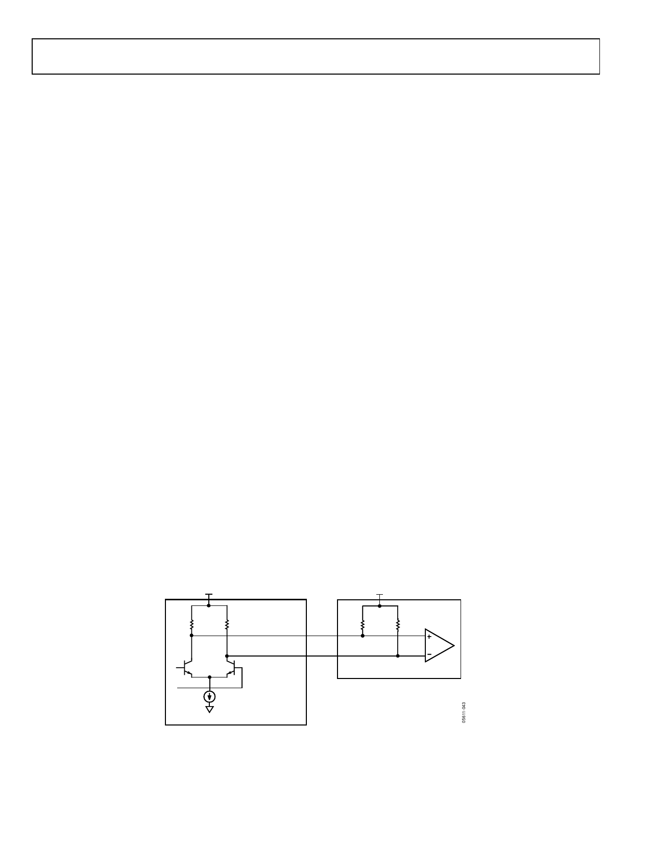
DC Coupling
First, consider the dc-coupled case (see Figure 44). A lane on
Output Port A or Output Port B on the AD8159 is dc-coupled
to a receiving device. In this example, the output termination
voltage (VTTO) on the AD8159 is set to the same level as the
input termination voltage (VTTIR) on the receiving device, and
this level sets the high value (VHI) of the single-ended output
voltage. With pre-emphasis low (PE = 0), the maximum single-
ended current is 16 mA1, which flows through the parallel
combination of the 50 Ω on-chip resistor and the 50 Ω far end
termination. Therefore, the low value (VLO) of the output
voltage is equal to
VTTO − 16 mA × (50 Ω || 50 Ω) = VTTO − 400 mV
Because the minimum allowed voltage at the output is
VCC − 1.6 V, the lowest acceptable value for VTTO is
VCC − 1.6 V + 0.4 V = VCC − 1.2 V
Increasing pre-emphasis to its highest level (PE = 3) results in
a maximum, single-ended current of 28 mA.2 In this case
VLO = VTTO − 28 mA × (50 Ω || 50 Ω) = VTTO − 700 mV
As a result, the lowest acceptable value for VTTO is
VCC − 1.6 V + 0.7 V = VCC − 0.9 V
It is expected that the minimum VTTO is 300 mV higher than the
case when PE = 0, because increasing the pre-emphasis level
results in a 300 mV lower voltage excursion at the output.
1 The output current for Port C when PE_C = 0 is slightly higher, 20 mA. The
extra 4 mA of current (compared to Port A/Port B) is needed to support the
bidirectional feature.
2 The output current for Port C when PE_C = 3 is 32 mA, for the same reason
as stated in Endnote 1.
VTTO
50Ω
50Ω
AD8159
OP
ON
VTTIR
RECEIVING DEVICE
PORT A/B: (16 + 4 × PE) mA
PORT C: (20 + 4 × PE) mA
VEE
Figure 44. DC-Coupling Output Signal from AD8159
Rev. A | Page 20 of 24
Share Link: 