P4C198 查看數據表(PDF) - Performance Semiconductor
零件编号
产品描述 (功能)
比赛名单
P4C198 Datasheet PDF : 13 Pages
| |||
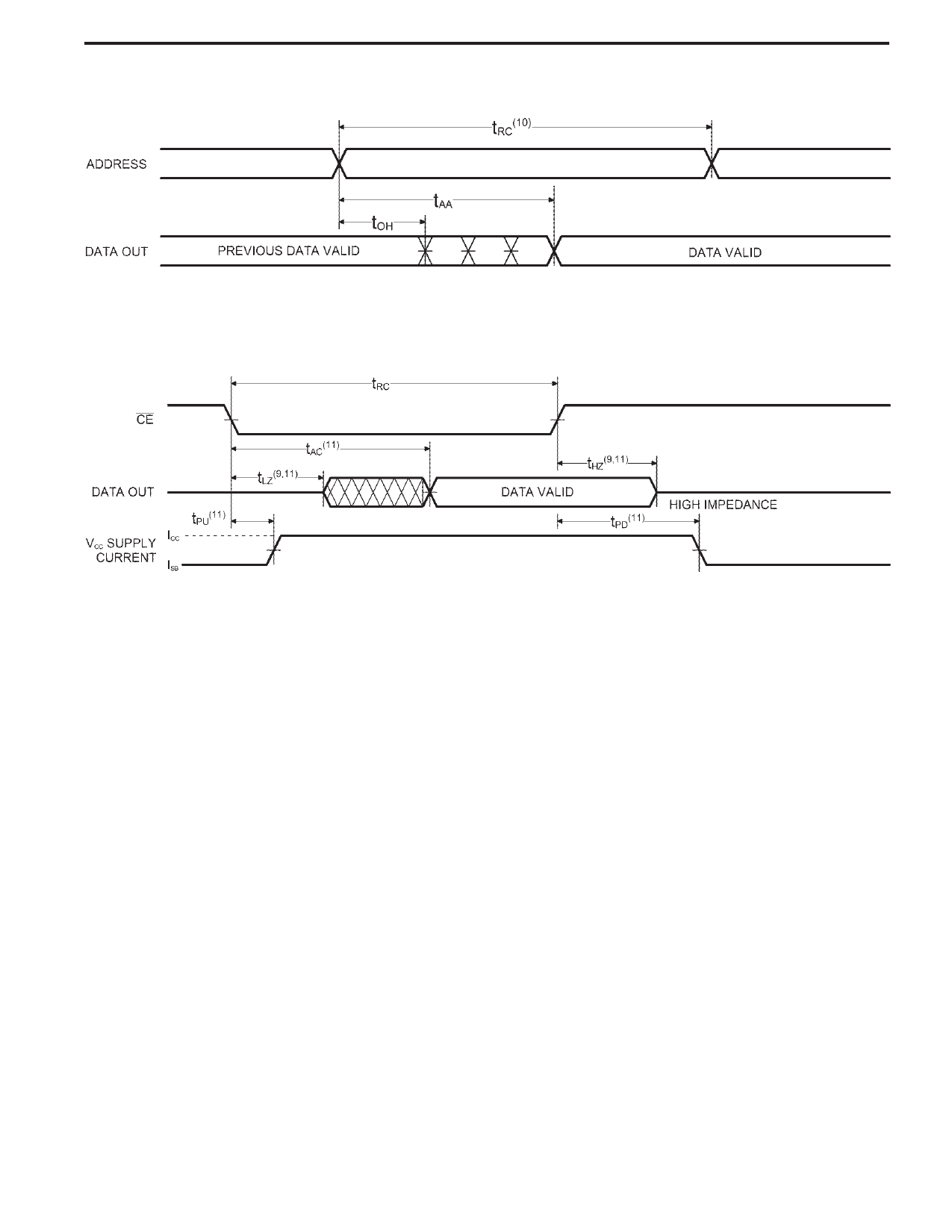
READ CYCLE NO. 2 (ADDRESS Controlled)(5,6)
P4C198/198L, P4C198A/198AL
READ CYCLE NO. 3 (CE(12) Controlled)(5,7,8)
Notes:
6. CE (CE1 CE2 for P4C198A/L) and OE are LOW READ cycle.
7. OE is LOW for the cycle.
8. ADDRESS must be valid prior to, or coincident with CE (CE1
and CE2 for P4C198A/L) transition LOW.
9. Transition is measured ± 200mV from steady state voltage
prior to change, with loading as specified in Figure 1.
10. Read Cycle Time is measured from the last valid address
to the first transitioning address.
11. Transitions caused by a chip enable control have similar
delays irrespective of whether CE1 or CE2 causes them
(P4C198A/L).
12. CE1, CE2 for P4C198A/L.
Document # SRAM113 REV A
Page 5 of 13
Share Link: 