P4C198L 查看數據表(PDF) - Performance Semiconductor
零件编号
产品描述 (功能)
比赛名单
P4C198L Datasheet PDF : 13 Pages
| |||
P4C198/198L, P4C198A/198AL
TRUTH TABLES
P4C198/L
CE WE OE
HX
X
LH H
LH
L
L
L
X
Mode
Standby
Output Inhibit
READ
WRITE
Output
High Z
High Z
DOUT
DIN
P4C198A/L
CE1 CE2 WE OE
HX
XX
XH
X
X
L
L
HH
L
L
HL
LL
LX
Mode
Standby
Standby
Output Inhibit
READ
WRITE
Output
High Z
High Z
High Z
DOUT
DIN
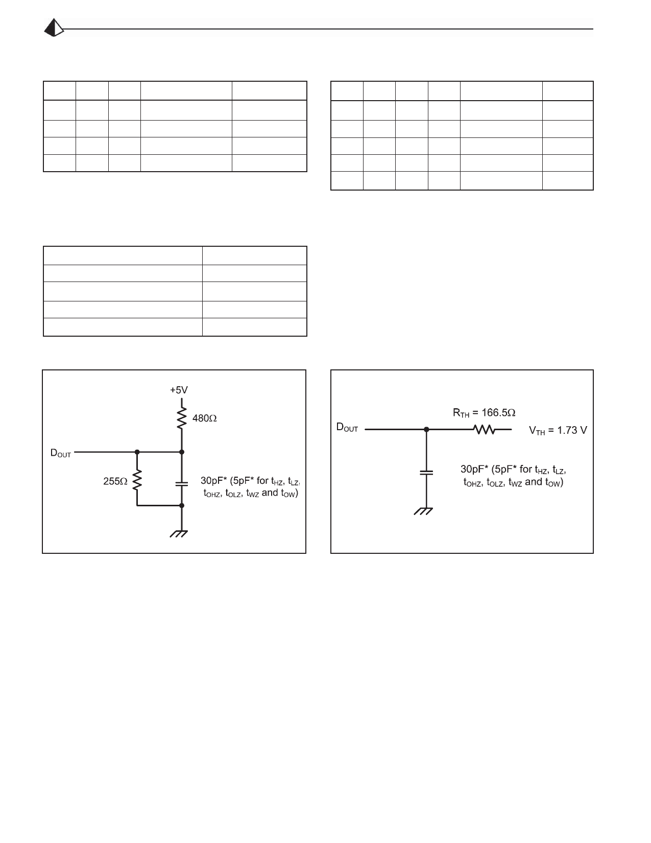
AC TEST CONDITIONS
Input Pulse Levels
Input Rise and Fall Times
Input Timing Reference Level
Output Timing Reference Level
Output Load
GND to 3.0V
3ns
1.5V
1.5V
See Figures 1 and 2
Figure 1. Output Load
* including scope and test fixture.
Note:
Because of the ultra-high speed of the P4C198/L and P4C198A/L, care
must be taken when testing this device; an inadequate setup can cause
a normal functioning part to be rejected as faulty. Long high-inductance
leads that cause supply bounce must be avoided by bringing the VCC and
ground planes directly up to the contactor fingers. A 0.01 µF high
Figure 2. Thevenin Equivalent
frequency capacitor is also required between VCC and ground. To avoid
signal reflections, proper termination must be used; for example, a 50Ω
test environment should be terminated into a 50Ω load with 1.73V
(Thevenin Voltage) at the comparator input, and a 116Ω resistor must
be used in series with DOUT to match 166Ω (Thevenin Resistance).
Document # SRAM113 REV A
Page 8 of 13
Share Link: 